|
|
PDF W25B40 Data sheet ( Hoja de datos )
| Número de pieza | W25B40 | |
| Descripción | 4M-BIT SERIAL FLASH MEMORY | |
| Fabricantes | Winbond | |
| Logotipo |  |
|
Hay una vista previa y un enlace de descarga de W25B40 (archivo pdf) en la parte inferior de esta página. Total 36 Páginas | ||
|
No Preview Available !
www.DataSheet4U.com
W25B40/W25B40A
4M-BIT SERIAL FLASH MEMORY
WITH BOOT AND PARAMETER SECTORS
Formally NexFlash NX25B40
The Winbond W25B40 / W25B40A is fully compatible with the previous NexFlash NX25B40 Serial
Flash memory.
Publication Release Date: January 6, 2006
- 1 - Revision M
1 page 
3. PIN CONFIGURATION
W25B40/W25B40A
Figure 1. W25B40 / W25B40A Pin Assignments, 8-pin SOIC (Package Code SN)
4. PIN DESCRIPTION
PIN NO.
1
2
3
4
5
6
7
8
PIN NAME
/CS
DO
/WP
GND
DI
CLK
/HOLD
VCC
I/O FUNCTION
I Chip Select Input
O Data Output
I Write Protect Input
Ground
I Data Input
I Serial Clock Input
I Hold Input
Power Supply
4.1 Package Types
The standard package for the W25B40 / W25B40A is an 8-pin plastic SOIC with 150-mil body
(Winbond package code SN) (NexFlash package code N). The pinout for the package is shown in
Figure 1. Package diagram and dimensions are illustrated at the end of this data sheet.
4.2 Chip Select (/CS)
The SPI Chip Select (/CS) pin enables and disables device operation. When /CS is high the device is
deselected and the Serial Data Output (DO) pin is at high impedance. When deselected, the devices
power consumption will be at standby levels unless an internal erase, program or status register cycle
is in progress. When /CS is brought low the device will be selected, power consumption will increase
to active levels and instructions can be written to and data read from the device. After power-up, /CS
must transition from high to low before a new instruction will be accepted. The /CS input must track
the VCC supply level at power-up (see “Write Protection” and figure 18). If needed a pull-up resister
on /CS can be used to accomplish this.
Publication Release Date: January 6, 2006
- 5 - Revision M
5 Page 
W25B40/W25B40A
write disable state occurs upon power-up or after any of the following instructions: Write Disable, Page
Program, Sector Erase, Chip Erase and Write Status Register.
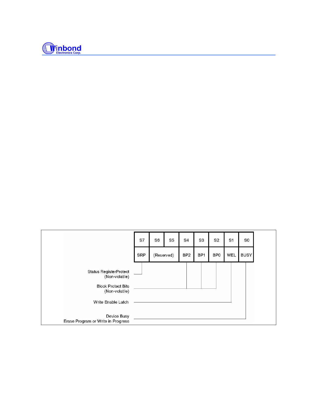
8.1.3 Block Protect Bits (BP2, BP1, BP0)
The Block Protect Bits (BP2, BP1, BP0) are non-volatile read/write bits in the status register (S4, S3,
S2) that provide Write Protection control and status. Block Protect bits can be set using the Write
Status Register Instruction (see tW in AC characteristics). All, none or a portion of the memory array
can be protected from Program and Erase instructions (see Status Register Memory Protection table).
The factory default setting for the Block Protection Bits is 0, none of the array protected. The Block
Protect bits can not be written to if the Status Register Protect (SRP) bit is set to 1 and the Write
Protect (/WP) pin is low.
8.1.4 Reserved Bits
Status register bit locations 5 and 6 are reserved for future use. Current devices will read 0 for these
bit locations. It is recommended to mask out the reserved bit when testing the Status Register. Doing
this will ensure compatibility with future devices.
8.1.5 Status Register Protect (SRP)
The Status Register Protect (SRP) bit is a non-volatile read/write bit in the status register (S7) that can
be used in conjunction with the Write Protect (/WP) pin to disable writes to the status register. When
the SRP bit is set to a 0 state (factory default) the /WP pin has no control over the status register.
When the SRP pin is set to a 1, the Write Status Register instruction is locked out while the /WP pin is
low. When the /WP pin is high the Write Status Register instruction is allowed.
Figure 3. Status Register Bit Locations
- 11 -
Publication Release Date: January 6, 2006
Revision M
11 Page | ||
| Páginas | Total 36 Páginas | |
| PDF Descargar | [ Datasheet W25B40.PDF ] | |
Hoja de datos destacado
| Número de pieza | Descripción | Fabricantes |
| W25B40 | 4M-BIT SERIAL FLASH MEMORY | Winbond |
| W25B40A | 4M-BIT SERIAL FLASH MEMORY | Winbond |
| Número de pieza | Descripción | Fabricantes |
| SLA6805M | High Voltage 3 phase Motor Driver IC. |
Sanken |
| SDC1742 | 12- and 14-Bit Hybrid Synchro / Resolver-to-Digital Converters. |
Analog Devices |
|
DataSheet.es es una pagina web que funciona como un repositorio de manuales o hoja de datos de muchos de los productos más populares, |
| DataSheet.es | 2020 | Privacy Policy | Contacto | Buscar |
