|
|
|
PDF WSF128K32-xH2x Data sheet ( Hoja de datos )
| Número de pieza | WSF128K32-xH2x | |
| Descripción | 128K x 32 SRAM/FLASH MODULE | |
| Fabricantes | White Electronic | |
| Logotipo | ||
Hay una vista previa y un enlace de descarga de WSF128K32-xH2x (archivo pdf) en la parte inferior de esta página. Total 12 Páginas | ||
|
No Preview Available !
www.DataSheet4U.com
White Electronic Designs
WSF128K32-XH2X
128KX32 SRAM/FLASH MODULE PRELIMINARY*
FEATURES
■ Access Times of 25ns (SRAM) and 70, 90 and 120ns
(FLASH)
■ Packaging:
66-pin, PGA Type, 1.385 inch square HIP, Hermetic
Ceramic HIP (Package 402)
■ 128Kx32 SRAM
■ 128Kx32 5V Flash
■ Organized as 128Kx32 of SRAM and 128Kx32 of
Flash Memory with common Data Bus
■ Low Power CMOS
■ Commercial, Industrial and Military Temperature Ranges
■ TTL Compatible Inputs and Outputs
■ Built-in Decoupling Caps and Multiple Ground Pins
for Low Noise Operation
■ Weight - 13 grams typical
FLASH MEMORY FEATURES
■ 10,000 Erase/Program Cycles
■ Sector Architecture
8 equal size sectors of 16K bytes each
Any combination of sectors can be concurrently
erased. Also supports full chip erase
■ 5 Volt Programming; 5V ± 10% Supply
■ Embedded Erase and Program Algorithms
■ Hardware Write Protection
■ Page Program Operation and Internal Program
Control Time.
* This data sheet describes a product under development, not fully
characterized, and is subject to change without notice.
Note: Programming information available upon request.
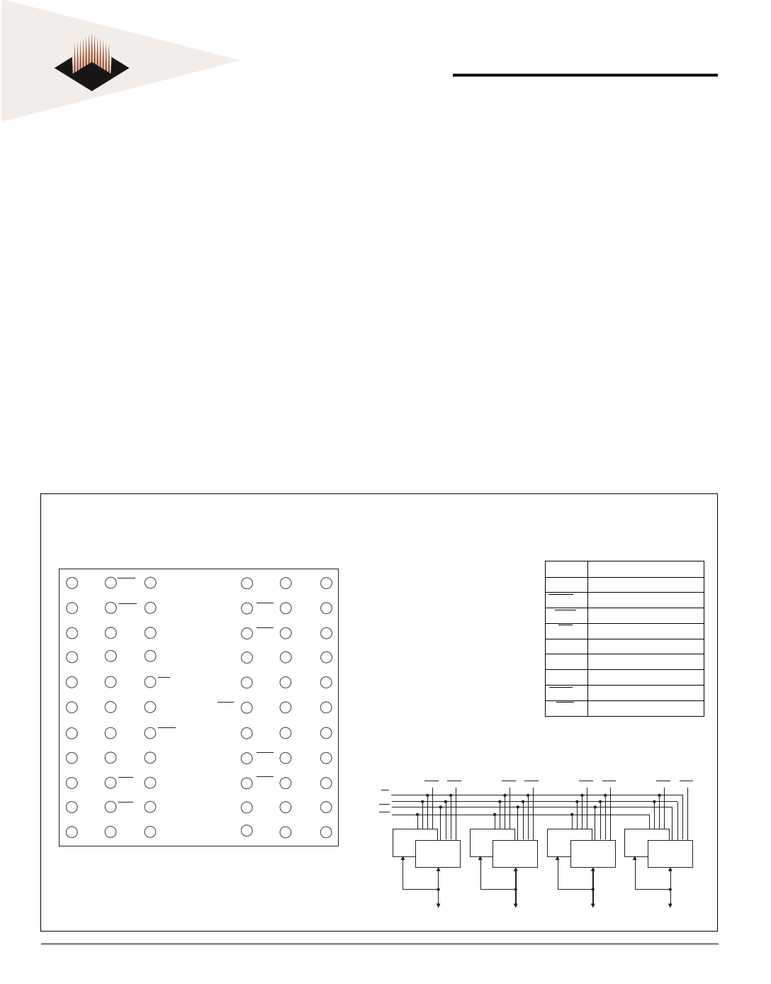
FIG. 1 PIN CONFIGURATION FOR WSF128K32-XH2X
TOP VIEW
1 12 23
34 45 56
I/O8 FWE2 I/O15
I/O24
VCC I/O31
I/O9 SWE2 I/O14
I/O25 SWE4
I/O30
I/O10
GND
I/O13
I/O26 FWE4
I/O29
A14
I/O11
I/O12
A7 I/O27
I/O28
A16 A10
OE
A12 A4
A1
A11 A9
NC
SWE1
A5
A2
A0 A15 FWE1
A13 A6
A3
NC VCC I/O7
A8 FWE3
I/O23
PIN DESCRIPTION
D0-31
A0-16
SWE1-4
SCS
OE
VCC
GND
NC
FWE1-4
FCS
Data Inputs/Outputs
Address Inputs
SRAM Write Enables
SRAM Chip Select
Output Enable
Power Supply
Ground
Not Connected
Flash Write Enables
Flash Chip Select
BLOCK DIAGRAM
I/O0 FCS I/O6
I/O1 SCS I/O5
I/O2 I/O3
I/O4
11 22
33
I/O16 SWE3
I/O22
I/O17 GND
I/O21
I/O18
I/O19
I/O20
44 55 66
OE
A0-16
SCS
FCS
FWE1 SWE1
FWE2 SWE2
FWE3 SWE3
FWE4 SWE4
128K x 8 Flash
128K x 8 SRAM
128K x 8 Flash
128K x 8 SRAM
128K x 8 Flash
128K x 8 SRAM
128K x 8 Flash
128K x 8 SRAM
October 2002 Rev. 4
I/O0-7
I/O8-15
I/O16-23
I/O24-31
1 White Electronic Designs Corporation (602) 437-1520 www.whiteedc.com
1 page 
White Electronic Designs WSF128K32-XH2X
FLASH AC CHARACTERISTICS WRITE/ERASE/PROGRAM OPERATIONS, FWE CONTROLLED
(VCC = 5.0V, TA = -55°C TO +125°C)
Parameter
Symbol
Write Cycle Time
Chip Select Setup Time
Write Enable Pulse Width
Address Setup Time
Data Setup Time
Data Hold Time
Address Hold Time
Chip Select Hold Time
Write Enable Pulse Width High
Duration of Byte Programming Operation (min)
Chip and Sector Erase Time
Read Recovery Time Before Write
VCC Set-up Time
Chip Programming Time
Output Enable Setup Time
Output Enable Hold Time (1)
tAVAV
tELWL
tWLWH
tAVWL
tDVWH
tWHDX
tWLAX
tWHEH
tWHWL
tWHWH1
tWHWH2
tGHWL
tWC
tCS
tWP
tAS
tDS
tDH
tAH
tCH
tWPH
tVCS
tOES
tOEH
-70
Min
70
0
35
0
30
0
45
0
20
14
2.2
0
50
0
10
Max
60
12.5
-90
Min Max
90
0
45
0
45
0
45
0
20
14
2.2 60
0
50
12.5
0
10
-120
Min Max
120
0
50
0
50
0
50
0
20
14
2.2 60
0
50
12.5
0
10
1. For Toggle and Data Polling.
Unit
ns
ns
ns
ns
ns
ns
ns
ns
ns
µs
sec
µs
µs
sec
ns
ns
FLASH AC CHARACTERISTICS READ ONLY OPERATIONS
(VCC = 5.0V, TA = -55°C TO +125°C)
Parameter
Symbol
Read Cycle Time
Address Access Time
Chip Select Access Time
OE to Output Valid
Chip Select to Output High Z (1)
OE High to Output High Z (1)
Output Hold from Address, FCS or OE Change,
whichever is first
1. Guaranteed by design, not tested.
tAVAV
tAVQV
tELQV
tGLQV
tEHQZ
tGHQZ
tAXQX
tRC
tACC
tCE
tOE
tDF
tDF
tOH
-70
Min
70
0
Max
70
70
35
20
20
-90
Min Max
90
90
90
40
25
25
0
-120
Min Max
120
120
120
50
30
30
0 ns
Unit
ns
ns
ns
ns
ns
ns
5 White Electronic Designs Corporation (602) 437-1520 www.whiteedc.com
5 Page 
White Electronic Designs WSF128K32-XH2X
FIG. 10 WRITE/ERASE/PROGRAM OPERATION FOR FLASH MEMORY, CS
CONTROLLED
NOTES:
1. PA represents the address of the memory location to be programmed.
2. PD represents the data to be programmed at byte address.
3. D7 is the output of the complement of the data written to the device.
4. DOUT is the output of the data written to the device.
5. Figure indicates the last two bus cycles of a four bus cycle sequence.
6. SCS = VIH
11 White Electronic Designs Corporation (602) 437-1520 www.whiteedc.com
11 Page | ||
| Páginas | Total 12 Páginas | |
| PDF Descargar | [ Datasheet WSF128K32-xH2x.PDF ] | |
Hoja de datos destacado
| Número de pieza | Descripción | Fabricantes |
| WSF128K32-xH2x | 128K x 32 SRAM/FLASH MODULE | White Electronic |
| Número de pieza | Descripción | Fabricantes |
| SLA6805M | High Voltage 3 phase Motor Driver IC. |
Sanken |
| SDC1742 | 12- and 14-Bit Hybrid Synchro / Resolver-to-Digital Converters. |
Analog Devices |
|
DataSheet.es es una pagina web que funciona como un repositorio de manuales o hoja de datos de muchos de los productos más populares, |
| DataSheet.es | 2020 | Privacy Policy | Contacto | Buscar |