|
|
|
PDF ADM1175 Data sheet ( Hoja de datos )
| Número de pieza | ADM1175 | |
| Descripción | Hot Swap Controller and Digital Power Monitor | |
| Fabricantes | Analog Devices | |
| Logotipo | ||
Hay una vista previa y un enlace de descarga de ADM1175 (archivo pdf) en la parte inferior de esta página. Total 25 Páginas | ||
|
No Preview Available !
Data Sheet
Hot Swap Controller and
Digital Power Monitor with Convert Pin
ADM1175
FEATURES
Allows safe board insertion and removal from
a live backplane
Controls supply voltages from 3.15 V to 16.5 V
Precision current sense amplifier
Precision voltage input
12-bit ADC for current and voltage readback
Charge pumped gate drive for external N-channel FET
Adjustable analog current limit with circuit breaker
±3% accurate hot swap current limit level
Fast response limits peak fault current
Automatic retry or latch-off on current fault
Programmable hot swap timing via TIMER pin
Active high and active low ON/ONB pin options
Convert start pin (CONV)
I2C fast mode-compliant interface (400 kHz maximum)
10-lead MSOP
APPLICATIONS
Power monitoring/power budgeting
Central office equipment
Telecommunications and data communications equipment
PCs/servers
GENERAL DESCRIPTION
The ADM1175 is an integrated hot swap controller and current
sense amplifier that offers digital current and voltage monitoring
via an on-chip, 12-bit analog-to-digital converter (ADC),
communicated through an I2C® interface.
An internal current sense amplifier measures voltage across
the sense resistor in the power path via the VCC pin and the
SENSE pin.
The ADM1175 limits the current through this resistor by
controlling the gate voltage (via the GATE pin) of an external
N-channel FET in the power path. The voltage across the sense
resistor (and, therefore, the inrush current) is kept below a
preset maximum.
The ADM1175 protects the external FET by limiting the time
that the maximum current runs through it. This current limit
period is set by the value of the capacitor attached to the TIMER
pin. Additionally, the device provides protection from overcurrent
events that may occur once the hot swap event is complete. In
the case of a short-circuit event, the current in the sense resistor
exceeds an overcurrent trip threshold, and the FET is switched
off immediately by pulling down the GATE pin.
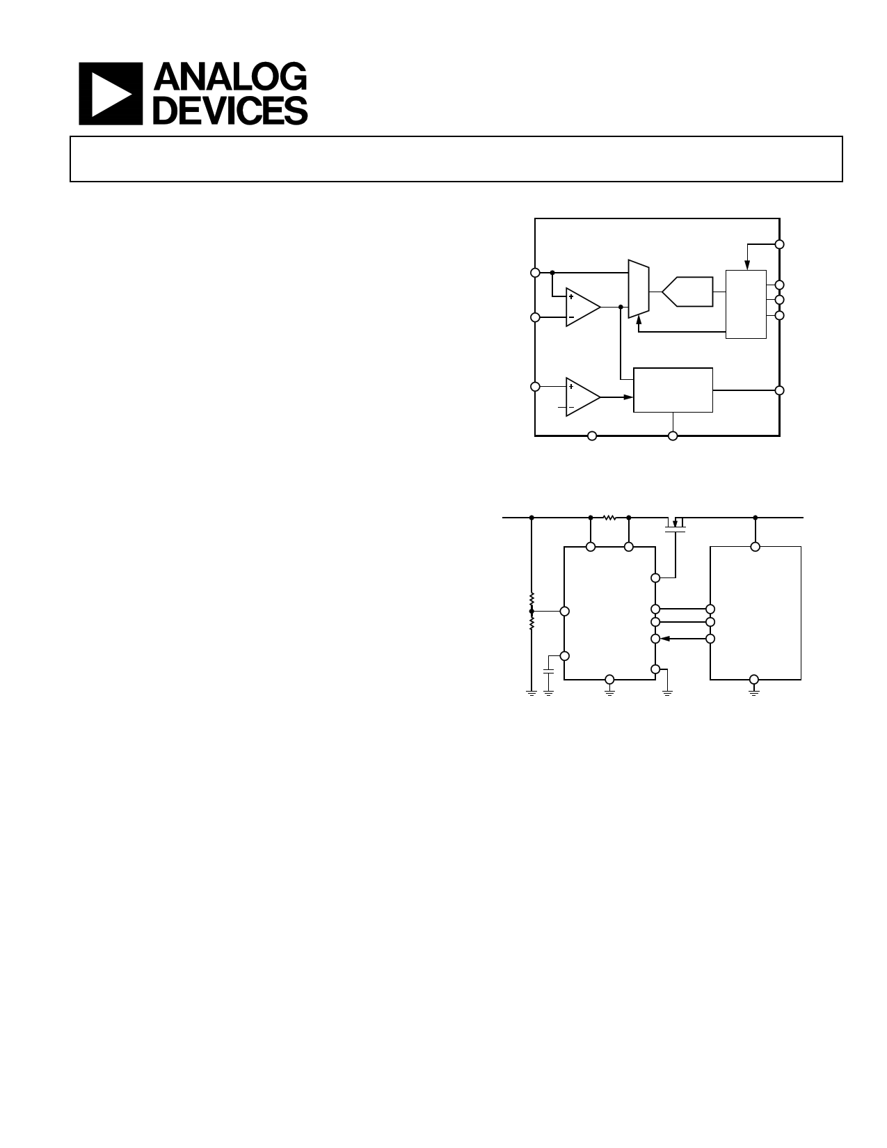
FUNCTIONAL BLOCK DIAGRAM
ADM1175-1
MUX
CONV
VCC
V
0
SENSE
I
A1
12-BIT
SDA
ADC
I2C SCL
ADR
CURRENT
SENSE
AMPLIFIER
ON
1.3V
UV COMPARATOR
GND
FET DRIVE
CONTROLLER
TIMER
Figure 1.
GATE
3.15V TO 16.5V
RSENSE N-CHANNEL FET
VCC SENSE
GATE
ADM1175-1
ON SDA
SCL
CONV
TIMER
GND ADR
CONTROLLER
P = VI
SDA
SCL
CONV
Figure 2. Applications Diagram
A 12-bit ADC can measure the current seen in the sense resistor,
as well as the supply voltage on the VCC pin. An industry-standard
I2C interface allows a controller to read current and voltage data
from the ADC. Measurements can be initiated by an I2C command
or via the convert (CONV) pin. The CONV pin is especially
useful for synchronizing reads on multiple ADM1175 devices.
Alternatively, the ADC can run continuously, and the user can
read the latest conversion data whenever it is required. Up to four
unique I2C addresses can be created, depending on how the ADR
pin is connected.
The ADM1175 is packaged in a 10-lead MSOP.
Rev. C
Information furnished by Analog Devices is believed to be accurate and reliable. However, no
responsibilityisassumedbyAnalogDevices for itsuse,nor foranyinfringementsofpatentsor other
rights of third parties that may result from its use. Specifications subject to change without notice. No
license is granted by implication or otherwise under any patent or patent rights of Analog Devices.
Trademarksandregisteredtrademarksarethepropertyoftheirrespectiveowners.
One Technology Way, P.O. Box 9106, Norwood, MA 02062-9106, U.S.A.
Tel: 781.329.4700
www.analog.com
Fax: 781.461.3113 ©2006–2012 Analog Devices, Inc. All rights reserved.
1 page 
ADM1175
Data Sheet
Parameter
MONITORING ACCURACY1
Current Sense Absolute Accuracy
0°C to +70°C
0°C to +85°C
−40°C to +85°C
VSENSE for ADC Full Scale2
Voltage Sense Accuracy
0°C to +70°C
0°C to +85°C
−40°C to +85°C
VCC for ADC Full Scale3
Low Range (VRANGE = 1)
High Range (VRANGE = 0)
I2C TIMING
Low Level Input Voltage, VIL
High Level Input Voltage, VIH
Low Level Output Voltage on SDA, VOL
Output Fall Time on SDA from VIHMIN to VILMAX
Maximum Width of Spikes Suppressed by
Input Filtering on SDA and SCL Pins
Input Current, II, on SDA/SCL When Not
Driving a Logic Low Output
Input Capacitance on SDA/SCL
SCL Clock Frequency, fSCL
Low Period of the SCL Clock
High Period of the SCL Clock
ADC Conversion Time4
Fast Overcurrent Response Time5
Setup Time for a Repeated Start Condition, tSU;STA
SDA Output Data Hold Time, tHD;DAT
Setup Time for a Stop Condition, tSU;STO
Bus Free Time Between a Stop and
a Start Condition, tBUF
Capacitive Load for Each Bus Line
Min Typ Max
−1.45
−1.8
−2.8
−5.7
−1.5
−1.8
−2.95
−6.1
−1.95
−2.45
−3.85
−6.7
105.84
+1.45
+1.8
+2.8
+5.7
+1.5
+1.8
+2.95
+6.1
+1.95
+2.45
+3.85
+6.7
−0.85
−0.9
−0.85
−0.9
−0.9
−1.15
+0.85
+0.9
+0.85
+0.9
+0.9
+1.15
6.65
26.35
0.7 VBUS
20 + 0.1 CBUS
50
−10
5
600
1300
600
100
600
1300
150
4
0.3 VBUS
0.4
250
250
+10
400
10
900
400
Unit
%
%
%
%
%
%
%
%
%
%
%
%
mV
%
%
%
%
%
%
V
V
V
V
V
ns
ns
µA
pF
kHz
ns
ns
µs
µs
ns
ns
ns
ns
pF
Conditions
VSENSE = 75 mV
VSENSE = 50 mV
VSENSE = 25 mV
VSENSE = 12.5 mV
VSENSE = 75 mV
VSENSE = 50 mV
VSENSE = 25 mV
VSENSE = 12.5 mV
VSENSE = 75 mV
VSENSE = 50 mV
VSENSE = 25 mV
VSENSE = 12.5 mV
VCC = 3 V minimum (low range)
VCC = 6 V minimum (high range)
VCC = 3 V minimum (low range)
VCC = 6 V minimum (high range)
VCC = 3 V minimum (low range)
VCC = 6 V minimum (high range)
VBUS = 3.0 V to 5.5 V
VBUS = 3.0 V to 5.5 V
IOL = 3 mA
CBUS = bus capacitance from SDA to GND
1 Monitoring accuracy is a measure of the error in a code that is read back for a particular voltage/current. This is a combination of amplifier error, reference error,
ADC error, and error in ADC full-scale code conversion factor.
2 This is an absolute value to be used when converting ADC codes to current readings; any inaccuracy in this value is factored into absolute current accuracy values (see
specifications for Current Sense Absolute Accuracy).
3 These are absolute values to be used when converting ADC codes to voltage readings; any inaccuracy in these values is factored into voltage accuracy values (see
specifications for Voltage Sense Accuracy).
4 Time between the receipt of the command byte and the actual ADC result being placed in the register.
5 Guaranteed by design; not production tested.
Rev. C | Page 4 of 24
5 Page 
ADM1175
120
115
110
105
100
95
90
85
80
2 4 6 8 10 12 14 16 18
VCC (V)
Figure 22. Circuit Breaker Limit Voltage vs. Supply Voltage
110
108
VOCFAST
106
104
102
VLIM
100
98 VOCTRIM
96
94
92
90
–40
–20
0
20 40 60
TEMPERATURE (°C)
Figure 23. VOCTRIM, VLIM, VOCFAST vs. Temperature
80
00
DECODE
3.2
3.0
2.8
2.6
2.4
2.2
2.0
1.8
1.6
1.4
1.2
1.0
0.8
0.6
0.4
0.2
0
–35 –30
–25
01
DECODE
–20 –15 –10
10 11
DECODE DECODE
–5 0
5 10
IADR (µA)
Figure 24. Address Pin Voltage vs. Address Pin Current
for Four Addressing Options
Data Sheet
1000
900
800
700
600
500
400
300
200
100
0
2046
2047
2048
CODE
2049
2050
Figure 25. ADC Noise with Current Channel, Midcode Input, and 1000 Reads
1000
900
800
700
600
500
400
300
200
100
0
779
780 781 782
CODE
783
Figure 26. ADC Noise with 14:1 Voltage Channel, 5 V Input, and 1000 Reads
1000
900
800
700
600
500
400
300
200
100
0
3078
3079
3080
CODE
3081
3082
Figure 27. ADC Noise with 7:1 Voltage Channel, 5 V Input, and 1000 Reads
Rev. C | Page 10 of 24
11 Page | ||
| Páginas | Total 25 Páginas | |
| PDF Descargar | [ Datasheet ADM1175.PDF ] | |
Hoja de datos destacado
| Número de pieza | Descripción | Fabricantes |
| ADM1170 | Hot Swap Controller | Analog Devices |
| ADM1171 | Hot Swap Controller | Analog Devices |
| ADM1172 | Hot Swap Controller | Analog Devices |
| ADM1173 | 2.7V to 16.5V Hot Swap Controller | Analog Devices |
| Número de pieza | Descripción | Fabricantes |
| SLA6805M | High Voltage 3 phase Motor Driver IC. |
Sanken |
| SDC1742 | 12- and 14-Bit Hybrid Synchro / Resolver-to-Digital Converters. |
Analog Devices |
|
DataSheet.es es una pagina web que funciona como un repositorio de manuales o hoja de datos de muchos de los productos más populares, |
| DataSheet.es | 2020 | Privacy Policy | Contacto | Buscar |