|
|
|
PDF IDT74AUC16373 Data sheet ( Hoja de datos )
| Número de pieza | IDT74AUC16373 | |
| Descripción | 1.8V CMOS 16-BIT TRANSPARENT D-TYPE LATCH WITH 3-STATE OUTPUTS | |
| Fabricantes | Integrated Device Technology | |
| Logotipo | ||
Hay una vista previa y un enlace de descarga de IDT74AUC16373 (archivo pdf) en la parte inferior de esta página. Total 7 Páginas | ||
|
No Preview Available !
www.DataSheet4U.com
IDT74AUC16373
1.8V CMOS 16-BIT TRANSPARENT D-TYPE LATCH WITH 3-STATE OUTPUTS
INDUSTRIALTEMPERATURERANGE
1.8V CMOS 16-BIT TRANSPARENT
D-TYPE LATCH WITH
3-STATE OUTPUTS
IDT74AUC16373
FEATURES:
• ESD > 2000V per MIL-STD-883, Method 3015; > 200V using
machine model (C = 200pF, R = 0)
• 1.8V Optimized
• 0.8V to 2.7V Operating Range
• Inputs/outputs tolerant up to 3.6V
• Output drivers: ±9mA @ 2.3V
• Supports hot insertion
• Available in TSSOP, TVSOP, and VFBGA packages
APPLICATIONS:
• high performance, low voltage communications systems
• high performance, low voltage computing systems
DESCRIPTION:
This 16-bit transparent D-type latch is built using advanced CMOS technol-
ogy. Thedevicecanbeusedasasingle16-bitlatchorastwo8-bitlatches. When
thelatchenable(LE)inputishigh,theQoutputsfollowthedata(D)inputs. When
LE is taken low, the Q outputs are latched at the levels set up at the D inputs.
A buffered output enable (OE) input can be used to place the eight outputs
in either a normal logic state (high or low logic levels) or a high-impedance state.
In the high-impedance state, the outputs neither load nor drive the bus lines
significantly. The OE input does not affect the internal operation of the latch.
This device is fully specified for partial power-down applications using IOFF.
The IOFF circuitry disables the outputs, preventing damaging current backflow
through the device when it is powered down.
To ensure the high-impedance state during power up or power down, OE
should be tied to VDD through a pull-up resistor; the minimum value of the resistor
is determined by the current-sinking capability of the driver.
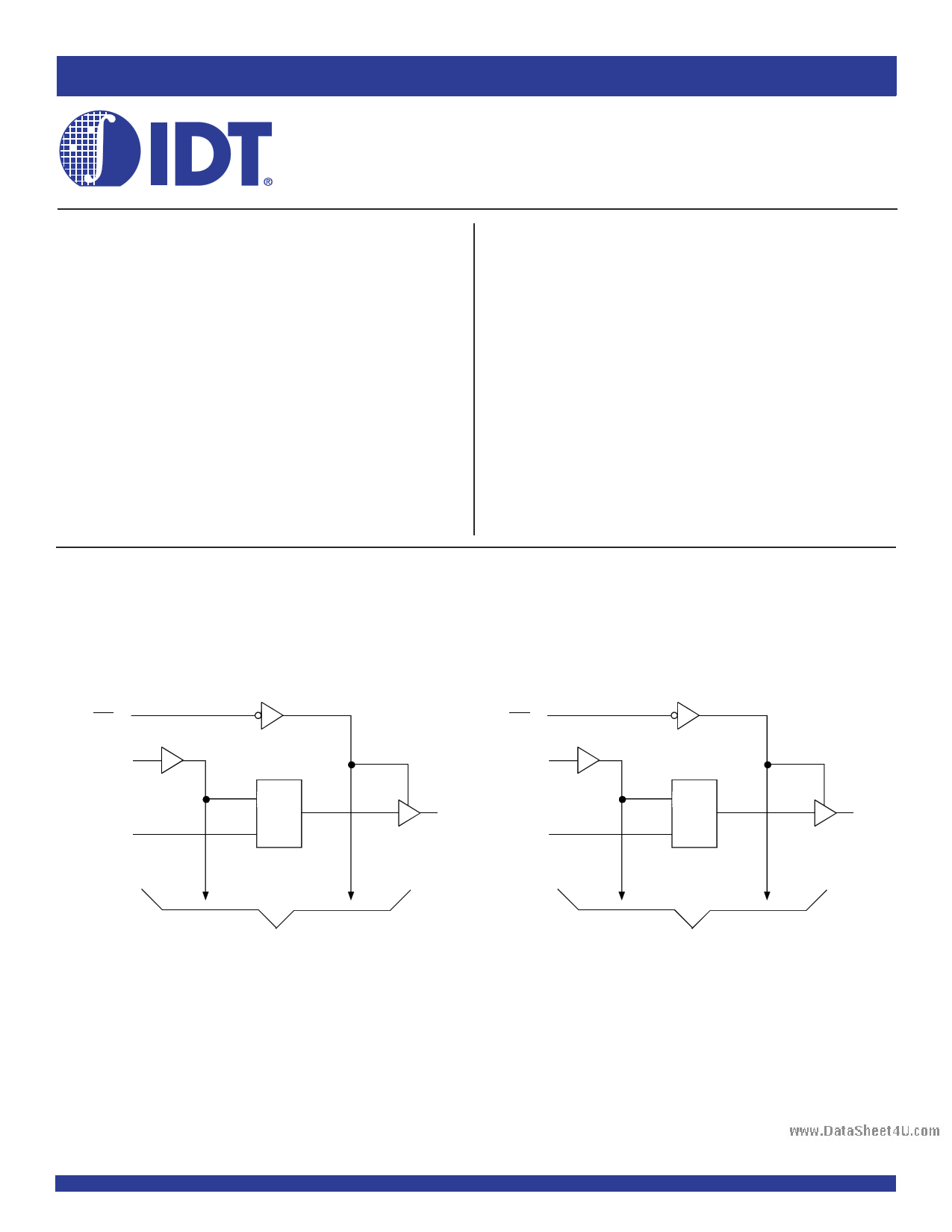
FUNCTIONAL BLOCK DIAGRAM
1OE
1LE
1D1
C1
1D
2OE
2LE
1Q1
2D1
C1
1D
2Q1
TO SEVEN OTHER CHANNELS
TO SEVEN OTHER CHANNELS
The IDT logo is a registered trademark of Integrated Device Technology, Inc.
INDUSTRIAL TEMPERATURE RANGE
© 2003 Integrated Device Technology, Inc.
DataSheet4 U .com
1
FEBRUARY 2003
DSC-6169/9
1 page 
www.DataSheet4U.com
IDT74AUC16373
1.8V CMOS 16-BIT TRANSPARENT D-TYPE LATCH WITH 3-STATE OUTPUTS
INDUSTRIALTEMPERATURERANGE
OUTPUT DRIVE CHARACTERISTICS
Symbol
VOH
Parameter
Output HIGH Voltage
VOL Output LOW Voltage
Test Conditions(1)
Min. Typ. Max. Unit
VDD = 0.8V - 2.7V
IOH = –100µA
VDD - 0.1
—
—
VDD = 0.8V
IOH = –0.7mA
—
0.55 —
VDD = 1.1V(2)
IOH = –3mA
0.8
—— V
VDD = 1.4V(3)
IOH = –5mA
1
——
VDD = 1.65V(4)
IOH = –8mA
1.2
——
VDD = 2.3V(5)
IOH = –9mA
1.8
——
VDD = 0.8V - 2.7V
IOH = 100µA
—
— 0.2
VDD = 0.8V
IOL = 0.7mA
—
0.25 —
VDD = 1.1V(2)
IOL = 3mA — — 0.3 V
VDD = 1.4V(3)
IOL = 5mA — — 0.4
VDD = 1.65V(4)
IOL = 8mA — — 0.45
VDD = 2.3V(5)
IOH = 9mA — — 0.6
NOTES:
1. VIL and VIH must be within the min. or max. range shown in the DC ELECTRICAL CHARACTERISTICS table for the appropriate VDD range. TA = -40°C to +85°C.
2. Demonstrates operation for nominal VDD = 1.2V.
3. Demonstrates operation for nominal VDD = 1.5V.
4. Demonstrates operation for nominal VDD = 1.8V.
5. Demonstrates operation for nominal VDD = 2.5V.
OPERATING CHARACTERISTICS, TA = 25°C
Symbol
CPD
CPD
Parameter
Power Dissipation Capacitance
Outputs Enabled
Power Dissipation Capacitance
Outputs Disabled
Test Conditions
CL = 0pF
f = 10MHz
VDD = 0.8V
21
5
VDD = 1.2V
22
5
VDD = 1.5V
23
6
VDD = 1.8V
25
7
VDD = 2.5V Unit
29 pF
10 pF
SWITCHING CHARACTERISTICS(1)
VDD = 0.8V VDD = 1.2V±0.1V
Symbol
tPLH
tPHL
tPZH
tPZL
tPHZ
tPLZ
tSU
tH
tW
Parameter
PropagationDelay xDx to xQx
xLE to xQx
Output Enable Time
xOE to xQx
Output Disable Time
xOE to xQx
Set-up Time, Data before LE↓
Hold Time, Data after LE↓
Pulse Duration, LE HIGH
Typ.
8
10.6
9
13
1.7
—
4.2
Min. Max.
1.1 3.8
1.4 4.9
1.3 4.5
2.4 7
0.7 —
1.2 —
2.9 —
NOTE:
1. See TEST CIRCUITS AND WAVEFORMS. TA = -40°C to +85°C.
VDD = 1.5V±0.1V
Min. Max.
0.6 2.4
0.7 3.2
0.6 2.9
2.4 4.8
0.5 —
0.8 —
2.3 —
VDD = 1.8V±0.15V
Min. Typ. Max.
0.7 1.5 2.4
0.7 1.6 2.8
0.8 1.7 2.9
1.1 2.7 4.6
0.4 — —
0.7 — —
2.1 — —
VDD = 2.5V±0.2V
Min. Max.
0.6 1.9
0.6 2.1
0.7 2.2
0.4 2.5
0.4 —
0.6 —
1.7 —
Unit
ns
ns
ns
ns
ns
ns
DataSheet4 U .com
5
5 Page | ||
| Páginas | Total 7 Páginas | |
| PDF Descargar | [ Datasheet IDT74AUC16373.PDF ] | |
Hoja de datos destacado
| Número de pieza | Descripción | Fabricantes |
| IDT74AUC16373 | 1.8V CMOS 16-BIT TRANSPARENT D-TYPE LATCH WITH 3-STATE OUTPUTS | Integrated Device Technology |
| Número de pieza | Descripción | Fabricantes |
| SLA6805M | High Voltage 3 phase Motor Driver IC. |
Sanken |
| SDC1742 | 12- and 14-Bit Hybrid Synchro / Resolver-to-Digital Converters. |
Analog Devices |
|
DataSheet.es es una pagina web que funciona como un repositorio de manuales o hoja de datos de muchos de los productos más populares, |
| DataSheet.es | 2020 | Privacy Policy | Contacto | Buscar |