|
|
|
PDF ICS9161A Data sheet ( Hoja de datos )
| Número de pieza | ICS9161A | |
| Descripción | Dual Programmable Graphics Frequency Generator | |
| Fabricantes | Integrated Circuit Systems | |
| Logotipo | ||
Hay una vista previa y un enlace de descarga de ICS9161A (archivo pdf) en la parte inferior de esta página. Total 15 Páginas | ||
|
No Preview Available !
www.DataSheet4U.com
Integrated
Circuit
Systems, Inc.
ICS9161A
Dual Programmable Graphics Frequency Generator
General Description
The ICS9161A is a fully programmable graphics clock
generator. It can generate user-specified clock frequencies
using an externally generated input reference or a single crystal.
The output frequency is programmed by entering a 24-bit
digital word through the serial port. Two fully user-
programmable phase-locked loops are offered in a single
package. One PLL is designed to drive the memory clock,
while the second drives the video clock. The outputs may be
changed on-the-fly to any desired frequency between 390 kHz
and 120 MHz. The ICS9161A is ideally suited for any design
where multiple or varying frequencies are required.
This part is ideal for graphics applications. It generates low
jitter, high speed pixel clocks. It can be used to replace multiple,
expensive high speed crystal oscillators. The flexibility of the
device allows it to generate non-standard graphics clocks.
Features
• Pin-for-pin and function compatible with ICD2061A
• Dual programmable graphics clock generator
• Memory and video clocks are individually
programmable on-the-fly
• Ideal for designs where multiple or varying frequencies
are required
• Increased frequency resolution from optional pre-
divide by 2 on the M counter
• Output enable feature available for tristating outputs
• Independent clock outputs range from 390 kHz to 120
MHz for VDD >4.75V
• Power-down capabilities
• Low power, high speed 0.8µ CMOS technology
• Glitch-free transitions
• Available in 16-pin, 300-mil SOIC or PDIP package
The ICS9161A is also ideal in disk drives. It can generate
zone clocks for constant density recording schemes. The low
profile, 16-pin SOIC or PDIP package and low jitter outputs
are especially attractive in board space critical disk drives.
The leader in the area of multiple output clocks on DaastianSglheeet4U.com
chip, ICS has been shipping graphics frequency generators
since October, 1990, and is constantly improving the phase-
locked loop. The ICS9161A incorporates a patented fourth
generation PLL that offers the best jitter performance available.
DataShee
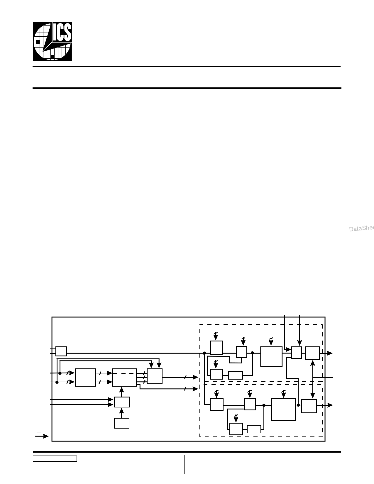
Block Diagram
EXTCLK EXTSEL
X1 XTAL
X2 OSC
SEL0-CLK
SEL1-DATA
INIT1
INIT2
24
ADDRESS CONTROL REG 21
VCLK
3 21 3-TO-1 (D0-D20) 21
24
DECODE
LOGIC
DATA
21
21
REGISTERS
MUX
21
MCLK
(D0-D20)
INIT
ROM
POR
PD
D14-D20
7
REF
fREF
DIVIDE
(M÷)
D4-D10
7
VCO
DIVIDE
(N÷)
D0-D3
4
VCO
Pscale
P= 2 or 4
D11-D13
3
VCO OUTPUT
DIVIDER
R=1,2,4,8,16
32,64,128
MUX
CMOS
OUTPUT
DRIVER
D14-D20
7
REF
DIVIDE
(M÷)
D0-D3
4
VCO
D4-D10
7
VCO
DIVIDE
(N÷)
Pscale
P= 2
D11-D13
3
VCO OUTPUT
DIVIDER
R=1,2,4,8,16
32,64,128
CMOS
OUTPUT
DRIVER
VCLK
OE
MCLK
DataSheet4U.com
9161-A RevG 10/04/00
9161
ICS reserves the right to make changes in the device data identified in this publication
without further notice. ICS advises its customers to obtain the latest version of all
device data to verify that any information being relied upon by the customer is current
and accurate.
1 page 
www.DataSheet4U.com
ICS9161A
Serial Programming Architecture
The pins SEL0 and SEL1 perform the dual functions of select-
ing registers and serial programming. In serial programming
mode, SEL0 acts as a clock pin while SEL1 acts as the data pin.
The ICS9161A-01 may not be serially programmed when in
power-down mode.
Since the VCLK registers are selected by the SEL0 and SEL1
pins, and since any change in their state may affect the output
frequency, new data input on the selection bits is only permitted
to pass through the decode logic after the watchdog timer has
timed out. This delay of SEL0 or SEL1 data permits a serial
program cycle to occur without affecting the current register
selection.
In order to program a particular register, an unlocking sequence
must occur. The unlocking sequence is detailed in the following
timing diagram:
Serial Data Register
The serial data is clocked into the serial data register in the
order described in Figure 1 below (Serial Data Timing).
The serial data is sent as follows: An individual data bit is
sampled on the rising edge of CLK. The complement of the
data bit must be sampled on the previous falling edge of CLK.
The setup and hold time requirements must be met on both
CLK edges. For specifics on timing, see the timing diagrams
on pages 10, 11 and 12.
et4U.com
The bits are shifted in this order: a start bit, 21 data bits, 3
The unlock sequence consists of at least five low-to-high address bits (which designate the desired register), and a stop
transitions of CLK while data is high, followed immediately bit. A total of 24 bits must always be loaded into the serial data
by a single low-to-high transition while data is low. Following register or an error is issued. Following the entry of the last
this unlock sequence, data can be loaded into the serial data data bit, a stop bit or load command is issued by bringing
register. This
in Figure 1.
programming
must
include
the
start
bitD, sahtoawSnheet4DTUhAe.TcAuonmhloigchkianngd
toggling CLK high-to-low and low-to-high.
mechanism then resets itself following the
load. Only after a time-out period are the SEL0 and SEL1 pins
Following any transition of CLK or DATA, the watchdog allowed to return to a register selection function.
timer is reset and begins counting. The watchdog timer
ensures that successive rising edges of CLK and DATA do not
violate the time-out specification of 2ms. If a time-out
occurs, the lock mechanism is reset and the data in the serial
data register is ignored.
DataShee
DataSheet4U.com
Figure 1: Serial Data Timing
5
5 Page 
www.DataSheet4U.com
ICS9161A
et4U.com
Selection Timing
DataSheet4U.com
DataShee
DataSheet4U.com
MCLK and Active VCLK Register Programming Timing
11
11 Page | ||
| Páginas | Total 15 Páginas | |
| PDF Descargar | [ Datasheet ICS9161A.PDF ] | |
Hoja de datos destacado
| Número de pieza | Descripción | Fabricantes |
| ICS9161A | Dual Programmable Graphics Frequency Generator | Integrated Circuit Systems |
| Número de pieza | Descripción | Fabricantes |
| SLA6805M | High Voltage 3 phase Motor Driver IC. |
Sanken |
| SDC1742 | 12- and 14-Bit Hybrid Synchro / Resolver-to-Digital Converters. |
Analog Devices |
|
DataSheet.es es una pagina web que funciona como un repositorio de manuales o hoja de datos de muchos de los productos más populares, |
| DataSheet.es | 2020 | Privacy Policy | Contacto | Buscar |