|
|
|
PDF DP83959 Data sheet ( Hoja de datos )
| Número de pieza | DP83959 | |
| Descripción | 8-Port Lite Ethernet Repeater Interface Controller | |
| Fabricantes | National Semiconductor | |
| Logotipo | ||
Hay una vista previa y un enlace de descarga de DP83959 (archivo pdf) en la parte inferior de esta página. Total 30 Páginas | ||
|
No Preview Available !
www.DataSheet4U.com
October 1997
DP83959
8-Port Lite Ethernet Repeater Interface Controller
General Description
Features
The DP83959 8-Port Lite Ethernet Repeater Interface s Fully IEEE 802.3 Ethernet Repeater compliant
Controller (LERIC8) is a single chip solution for unman- s Eight IEEE 802.3 10BASE-T compliant ports with
aged 10BASE-T Ethernet repeater (hub) products. By inte-
on-chip transmit filters
grating electronics needed to support eight 10BASE-T s One IEEE 802.3 compatible AUI port
ports, a full level/drive compatible AUI port for a backbone s Direct drive status LED outputs
connection, and an internal power on reset circuit, a s Network traffic level monitor with direct drive LED
LERIC8 based design requires only the addition of a few
outputs
passive components: crystal, transformers, connectors s Automatic internal power-on reset function. External
and a power source.
TTL compatible reset pin provided for device testing if
The LERIC8 provides on-chip LED drivers that connect di-
rectly to LEDs via series resistors. In addition to the Link
OK, Port Partition, Global Activity and Global Collision LED
outputs, the LERIC8 provides an on chip network traffic
level monitor circuit with 8 LED outputs to drive a bargraph
type display.
The LERIC8 also provides an LED and Inter Repeater Bus
interface that is compatible with the DP83955/6 LERIC™
products.
required
s Inter-LERIC™ bus for cascading up to 3 devices on a
single board
s Register/LED status interface compatible with
DP83955/6 LERIC™ products
s Single 20 MHz crystal or external 20 MHz oscillator
module operation
s Single 5V supply
s 160 pin PQFP package
DataSheet4U.com
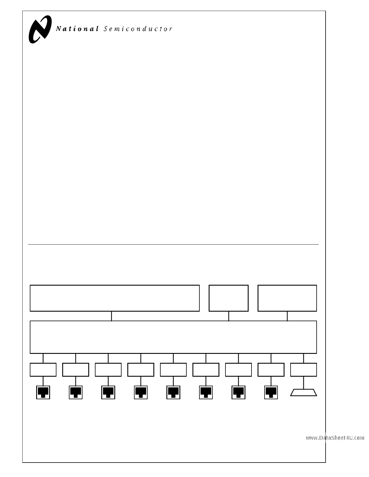
1.0 System Diagram
DataShee
Status LEDs (Optional)
Per 10BASE-T Port Link & Partition
AUI Port Partition
Global Activity, Global Collision
Network Traffic Bargraph
Alert (High Traffic or Long Partition)
20MHz
Oscillator
or Crystal
Inter Repeater Bus
(Optional)
DP83959 LERIC8
8-Port Lite Ethernet Repeater Interface Controller
Transformer
Transformer
Transformer
Transformer
Transformer
Transformer
Transformer
Transformer
Transformer
10BASE-T
Port 1
10BASE-T
Port 2
10BASE-T
Port 3
10BASE-T
Port 4
10BASE-T
Port 5
10BASE-T
Port 6
10BASE-T
Port 7
10BASE-T
Port 8
AUI
Port
DataSheet4U.com
TRI-STATE® is a registered trademark of National Semiconductor Corporation.
LERIC™ and Inter-LERIC™ are trademarks of National Semiconductor Corporation.
©1997 National Semiconductor Corporation
DataSheet4 U .com
www.national.com
1 page 
www.DataSheet4U.com
et4U.com
4.0 Pin Descriptions
Key to Pin Type:
O = TTL Compatible Output
O (ECL) = ECL Compatible Output
I = TTL Compatible Input
I (ECL) = ECL Compatible Input
OZ = TTL Compatible TRI-STATE® Output
O (O.D.) = Open Drain Output
4.1 AUI PORT (PORT 0)
I/O = TTL Compatible Input/Output
I/O (O.D.) = TTL Compatible Input/Open Drain Output
TPO = Twisted Pair Interface Compatable Output
TPI = Twisted Pair Interface Compatable Input
AI = Analog Input
Signal Name Type Pin #
Description
TX0+
O
(ECL)
68 AUI Transmit +: The AUI transmit path includes National Semiconductor's
patented low power dissipation differential drivers that do not need external load
resistors. This output should be connected directly to the AUI isolation transformer.
TX0-
O
(ECL)
69 AUI Transmit -: The AUI transmit path includes National Semiconductor's patented
low power dissipation differential drivers that do not need external load resistors.
This output should be connected directly to the AUI isolation transformer.
RX0+
I
(ECL)
72 AUI Receive +: This input should be terminated with 39Ω to GND via a series DC
blocking capacitor (shared with RX0-). Refer to Figure 8.
RX0-
I
(ECL)
73 AUI Receive -: This input should be terminated with 39Ω to GND via a series DC
blocking capacitor (shared with RX0+). Refer to Figure 8.
CD0+
I
(ECL)
70 AUI Collision Detect +: This input should be terminated with 39Ω to GND via a
series DC blocking capacitor (shared with CD0-). Refer to Figure 8.
CD0-
I
(ECL)
71 AUI Collision Detect -: This input should be terminated with 39Ω to GND via a
series DC blocking capacitor (shared with CD0+). Refer to Figure 8.
DataSheet4U.com
4.2 TWISTED PAIR PORTS (PORTS 1 - 8)
Signal Name
REQ
RTX
Type
AI
AI
Pin #
108
107
Description
Equalization Resistor: A resistor connected between this pin and GND or VCC
adjusts the equalization step amplitude on the 10BASE-T Manchester encoded
transmit data for all eight 10BASE-T ports. No resistor is required for operation with
cable length of up to 100 meters.
Extended Cable Resistor: A resistor connected between this pin and GND or VCC
adjusts the amplitude of the differential transmit outputs for all eight 10BASE-T
ports. No resistor is required for operation with cable length of up to 100 meters.
DataShee
DataSheet4U.com
DataSheet4 U .com
5
www.national.com
5 Page 
www.DataSheet4U.com
et4U.com
4.0 Pin Descriptions (Continued)
4.6 REGISTER/CONFIGURATION INTERFACE
Signal Name
RA4
RA3
RA2
RA1
RA0
D3
D2
D1
D0
/RD
/WR
/READY
/STR
DFS
BUFEN
/MLOAD
Type
I/O
I/O
I
I
O
O
O
O
I
Pin #
63
62
61
60
59
56
55
54
53
31
30
51
36
37
52
142
Description
Register Address [4:0]: Address input value for the current register access.
These pins also provide DP83955/6 compatible LED status: during display
update cycles these pins become outputs that provide port address and data
for LED display purposes. Pins RA[1:4] cycle values from 0h to 9h while RA0
provides Bad Polarity status for the 10BASE-T ports. See Section 5.13 for
more details. If the DP83955/6 compatible LEDs and register interface are not
being used, these pins should be left unconnected.
In Option mode (see DEF/OPT), the logic levels present on RA[4:0] at reset
(set by pull-up or pull-down resistors) are latched into the configuration
registers. See section 5.12 for more information.
Data [3:0]: Bi-directional register data. /RD and /WR control the data
direction. With /RD low and /WR high, D[3:0] are outputs and with /RD high
and /WR low, D[3:0] are inputs. These pins also provide the DP83955/6
compatible status outputs for latching to LEDs. See Section 5.13 for more
details. If the DP83955/6 compatible LEDs and register interface are not being
used, these pins should be left unconnected.
In Option mode (see DEF/OPT), the logic levels present on D[3:0] at reset (set
by pull-up or pull-down resistors) are latched into the configuration registers.
See Section 5.12 for more information.
Read Strobe: When strobed low, this input schedules a register read access
to the register addressed by the RA[4:0] pins. If the register interface is not
being used, this pin should be connected to VCC either directly or via a pull-up
resistor (≈4.7 kΩ).
Write
to the
DSretargtoiasbSteeh:r eWaedhtd4erUnes.scstreoodmbebdy
low,
the
this input schedules a register write access
RA[4:0] pins. If the register interface is not
being used, this pin should be connected to VCC either directly or via a pull-up
resistor (≈4.7 kΩ).
Ready Handshake: The falling edge of this active low signal during a read
cycle indicates that data is stable and valid for sampling. In write cycles, the
falling edge of /READY denotes that the write data has been latched by the
LeRIC8. Therefore, data must have been available and stable for this
operation to be successful.
Display Update Strobe: When using the DP83955/6 compatible status LEDs,
this active low signal controls the latching of display data for network ports into
the external display latches. If not required, this pin should be left
unconnected.
Display Frozen Strobe: Asserted high when the display data for each packet
is frozen at the end of the repeater transmission of the packet until the start of
the next network event or for a maximum of 30ms (nominal value). This
ensures DP83955/6 compatible status LEDs are visible even for single
network events.
Buffer Enable: Used to control an external buffer (if required) for the data
bus, D[3:0]. Extermal buffer will be necessary in systems having a register
interface.
Mode Load/Reset: TTL level reset input (not Schmitt) for external reset or
test purposes. If not required, this pin should be connected to VCC either
directly or via a pull-up resistor (≈4.7 kΩ). On the rising (trailing) edge of
/MLOAD, the logic levels present on the D[3:0] and RA[4:0] inputs (set by
pull-up or pull-down resistors) are latched into the configuration registers.
DataShee
DataSheet4U.com
DataSheet4 U .com
11 www.national.com
11 Page | ||
| Páginas | Total 30 Páginas | |
| PDF Descargar | [ Datasheet DP83959.PDF ] | |
Hoja de datos destacado
| Número de pieza | Descripción | Fabricantes |
| DP83950B | DP83950B RIC Repeater Interface Controller (Rev. A) | Texas Instruments |
| DP83950B | Repeater Interface Controller | National Semiconductor |
| DP83952 | DP83952 Repeater Interface Controller with Security Features (RIC II) (Rev. A) | Texas Instruments |
| DP83952 | Repeater Interface Controller with Security Features | National Semiconductor |
| Número de pieza | Descripción | Fabricantes |
| SLA6805M | High Voltage 3 phase Motor Driver IC. |
Sanken |
| SDC1742 | 12- and 14-Bit Hybrid Synchro / Resolver-to-Digital Converters. |
Analog Devices |
|
DataSheet.es es una pagina web que funciona como un repositorio de manuales o hoja de datos de muchos de los productos más populares, |
| DataSheet.es | 2020 | Privacy Policy | Contacto | Buscar |