|
|
|
PDF TB31296FT Data sheet ( Hoja de datos )
| Número de pieza | TB31296FT | |
| Descripción | Bluetooth RF IC | |
| Fabricantes | Toshiba Semiconductor | |
| Logotipo | ||
Hay una vista previa y un enlace de descarga de TB31296FT (archivo pdf) en la parte inferior de esta página. Total 9 Páginas | ||
|
No Preview Available !
www.DataSheet4U.com
Preliminary
TB31296FT
TOSHIBA SiGe-BiCMOS LINEAR INTEGRATED CIRCUIT SILICON MONOLITHIC
TB31296FT
Bluetooth RF IC
FEATURES
BlueRF RXMODE1
Power Consumption TX mode 27.0mA (Typ.)
RX mode 42.0mA (Typ.)
Operating Voltage Range 2.7V ~ 3.5 V
Small Package FBGA 48in
Build-in LNA
Build-in VCO
Build-in PA 0dBm output ( typ. controllable)
External PA control voltage supply for Class1
Very slight current consumption in Deep Sleep mode
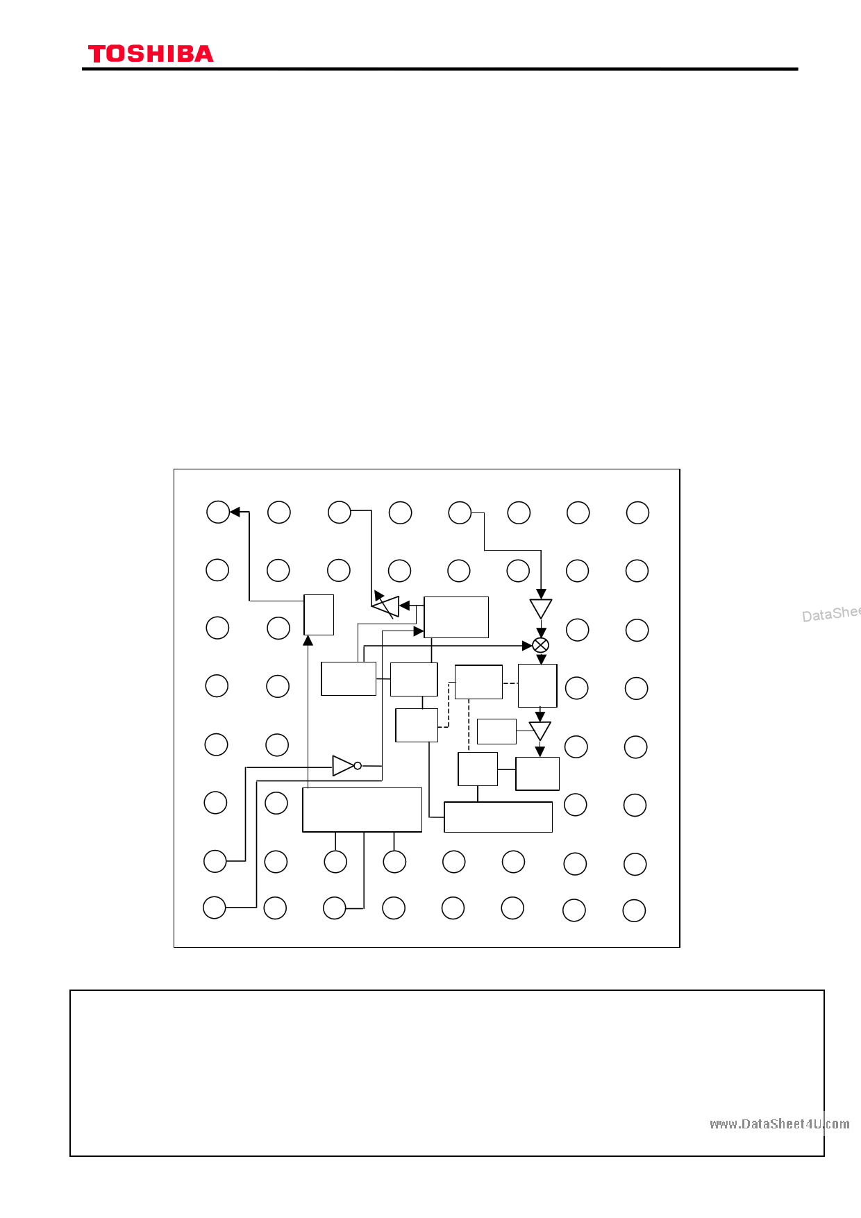
BLOCK DIAGRAM
PA_CONT GNDTX1 TXout
VccTX
RXin GNDRXPA1 MIX_C MIXout
ANTSW
LFIL1
ANTSWX GNDTX2
DA
VccVCO C
NC VccRX GNDRXPA2
LNA
DataSheet4PUL.Lcom
MIX
NC
VccIF1
Iref1
IFref2
GNDVCO ResetX
LD NC
Doubler
VCO
TXLPF
FLLLPF
BPF
FLLRC
RSSI
LPF
FLLGC
DET
GNDIF1
AFout
Serial data cont.
BSX
VccPLL
ADC
GNDIF2
Cin
DataShee
XOin
GNDPLL2 SSTB
SDATA
RFbus1
RFbus2
PASW
LFIL2
XOout
Vdd
SCLK GNDPLL1 Cout
BB13M
RSSI
VccIF2
(Top View)
The information contained herein is subject to change without notice.
-The information contained herein is presented only as a guide for the applications of our products. No responsibility is assumed by
TOSHIBA for any infringements of patents or other rights of the third parties which may result from its use. No license is granted by
implication or otherwise under any patent or patent rights of TOSHIBA or others.
-TOSHIBA is continually working to improve the quality and the reliability of its products. Nevertheless, semiconductor devices in general
can malfunction or fail due to their inherent electrical sensitivity and vulnerability to physical stress. It is the responsibility of the buyer, when
utilizing TOSHIBA products, to observe standards of safety, and to avoid situations in which a malfunction or failure of a TOSHIBA product
could cause loss of human life, bodily injury or damage to property.
In developing your designs, please ensure that TOSHIBA products are used within specified operating ranges as set forth in the most
DataSheet4UrRe.eccleoianmbtiliptyroHdauncdtsbosopke.cifications. Also, please keep in mind the precautions and conditions set forth in the TOSHIBA Semiconductor
-The products described in this document may include products subject to the foreign exchange and foreign trade laws.
-1-
June 26, 2003-
DataSheet4 U .com
1 page 
www.DataSheet4U.com
TENTATIVE
4 MAXIMUM RATINGS ( Ta=25 )
CHARACTERISTICS
SYMBOL
RATING UNIT
Power Supply Voltage
Power Dissipation
Input terminal Voltage
Storage Temperature Range
VCC
PD
CLK DATA STB BS LD
Tstg -50
3.6 V
530 mW
3.4 V
150
Maximum ratings indicate the limits, which the device must not be beyond
TB31296FT
5 OPERATING RANGES
CHARACTERISTICS
SYMBOL TEST CONDITION
MIN TYP. MAX UNIT
Analog supply voltage
Vcc*
2.7 3.3 3.4 V
Digital interface I/O supply voltage Vdd
1.8 3.3 3.4 V
Operating temperature
Topr
-35 85
Operating ranges indicate the conditions for which the device is intended to be functional even with the electrical changes
6 ELECTRICAL CHARACTERISTICS ( Unless otherwise specified, Ta=25 ,VCC=3.3V , f=2450MHz)
This spec is IC design target value and in mass production these may be updated.
et4U.com
POWER SUPPLY
CHARACTERISTICS
Current Consumption Rx (*2)
Current Consumption Tx
Current Consumption tune
Current Consumption BS
" H " level input/output level
" L " level input/output level
SYMBOL
ICCRX
ICCTX
ICCwait2
ICC BS
VIH
VIL
TEST CONDITION
MIN TYP. MAX UNIT
RX mode, BS=H
- 42.0 60.0 mA
TX mode, BS=H, PAout=0[dBm]
- 26.9 40.0 mA
During synthesizer tuning
- 15.5
- mA
BaDtteartyaSsahveeemt4oUd.ec,oBmS=L
-
0.01 10 uA
CLK, DATA, STB, BS, RFbus1, Vdd
RFbus2, BB13M
0.8
Vdd Vdd+ V
0.2
CLK, DATA, STB, BS, RFbus1,
RFbus2, BB13M
-0.2
0 Vdd V
0.2
DataShee
INPUT SIGNAL REGURATION
CHARACTERISTICS
Reference Clock frequency
Reference Clock level
Serial data bus input frequency
SYMBOL
Fclk
Vclk
Dbus-freq.
TEST CONDITION
200[kHz] step
MIN TYP. MAX UNIT
4 13 50 MHz
TBD 110 TBD dBuV
- 13 20 MHz
PLL CHARACTERISTICS
CHARACTERISTICS
Operating frequency range
Lock Up Time
VCO phase noise
SYMBOL
t-lock
Pn1
Pn2
Pn3
TEST CONDITION
Phase comparison ref: 500kHz
CP current= 2mA
@500kHz
@1MHz
@2MHz
MIN TYP. MAX UNIT
2380
-
2500 MHz
85 - us
107 dBc/Hz
113 dBc/Hz
119 dBc/Hz
DataSheet4U.com
DataSheet4 U .com
-5-
June 26, 2003
5 Page | ||
| Páginas | Total 9 Páginas | |
| PDF Descargar | [ Datasheet TB31296FT.PDF ] | |
Hoja de datos destacado
| Número de pieza | Descripción | Fabricantes |
| TB31296FT | Bluetooth RF IC | Toshiba Semiconductor |
| Número de pieza | Descripción | Fabricantes |
| SLA6805M | High Voltage 3 phase Motor Driver IC. |
Sanken |
| SDC1742 | 12- and 14-Bit Hybrid Synchro / Resolver-to-Digital Converters. |
Analog Devices |
|
DataSheet.es es una pagina web que funciona como un repositorio de manuales o hoja de datos de muchos de los productos más populares, |
| DataSheet.es | 2020 | Privacy Policy | Contacto | Buscar |