|
|
PDF L24W08 Data sheet ( Hoja de datos )
| Número de pieza | L24W08 | |
| Descripción | (L24W04 / L24W08) Serial EEPROM | |
| Fabricantes | Link Smart | |
| Logotipo |  |
|
Hay una vista previa y un enlace de descarga de L24W08 (archivo pdf) en la parte inferior de esta página. Total 14 Páginas | ||
|
No Preview Available !
www.DataSheet4U.com
L24W04/08
Serial EEPROM
DataSheet4U.com
Data Sheet
Revision A
DataShee
DataSheet4U.com
DataSheet4 U .com
S062A
1 page 
www.DataSheet4U.com
LinkSmart
L24W04/08
4K/8K 2-Wire (512x8/1,024x8)
3V~5.5V CMOS Serial EEPROM
PRELIMINARY
A
et4U.com
Functional Description
z Serial clock (SCL)
The SCL input is used for positive edge clock
data into each EEPROM device and negative
edge clock data out of each device.
z Serial data (SDA)
The SDA pin is bidirectional for serial data
transfer. The pin is open drain driven and may
be wired-OR with any number of other open
drain or open collector devices.
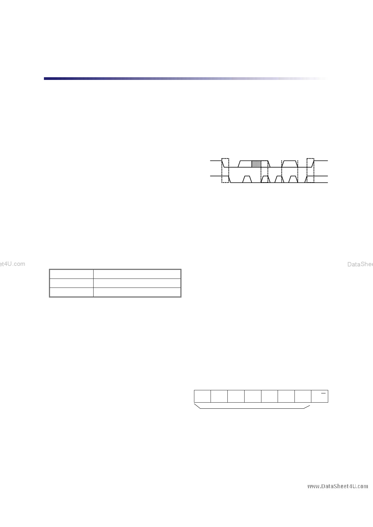
standby power mode (refer to Start and Stop
Definition Timing Diagram).
z Acknowledge
All addresses and data words are serially
transmitted to and from the EEPROM in 8-bit
words. The EEPROM sends a zero to
acknowledge that it has received each word.
This happens during the ninth clock cycle.
Date allowed
to change
SDA
z A0, A1, A2
The L24W04/08 uses the A2 input for hard wire
addressing and a total of two 8K devices may
be addressed on a single bus system. The A0
and A1 pins have no connection.
SCL
Start Address or
condition acknowledge
valid
No ACK Stop
state condition
Device Addressing
z Write protect (WP)
The 4K/8K EEPROM device requires an 8-bit
The L24W04/08 has a write protect pin that
device address word following a start condition
provides hardware data protection. The write
to enable the chip for a read or write operation.
protect pin allows normal read/write operations
The device address word consists of a
when the connection is grounded. When the
mandatory one, zero sequence for the first four
write protect pin is connected to Vcc, the write
most significant bits (refer to the diagram
protection feature is enabled
shown in the following table.
and
operaDteastaaSsheet4Usa.chllooEmwEinPgRtOheMDdeevviicceesA.ddress).
This
is
common
to
WP Pin Status
Protect Array
At Vcc
Full Array (4K/8K)
At Vss
Normal Read/Write operations
The 4K/8K EEPROM uses the A2 device
address bit with the next two bits for memory
page addressing. The A2 bit must compare its
corresponding hard-wired input pin. The A1 and
A0 pins have no connection.
Memory Organization
Internally organized with 512/1,024 8-bit words,
the 4K/8K requires a 10-bit data word address
for random word addressing.
These page addressing bits on the 8K device
should be considered the most significant bits of
the data word address which follows. The A0, A1
and A2 pins have no connection.
The 8th bit device address is the read/write
Device Operations
z Clock and data transition
Data transfer may be initiated only when the
bus is not busy. During data transfer, the data
line must remain stable whenever the clock line
is high. Changes in data line while the clock
line is high will be interpreted as a START or
operation select bit. A read operation is initiated
if this bit is high and a write operation is initiated
if this bit is low.
If the comparison of the device address
succeeds the EEPROM will output a zero at
ACK bit. If not, the chip will return to a standby
state.
STOP condition.
10
1 0 A2 A1 A0 R/W
z Start condition
A high-to-low transition of SDA with SCL high is
a start condition which must precede any other
command (refer to Start and Stop Definition
Timing diagram).
z Stop condition
A low-to-high transition of SDA with SCL high is
a stop condition. After a read sequence, the
stop command will place the EEPROM in a
Device Address
Write Operations
z Byte write
A write operation requires an 8-bit data word
address following the device address word and
acknowledgment. Upon receipt of this address,
the EEPROM will again respond with a zero
DataSheet4U.com
5 2004/4/26
DataShee
DataSheet4 U .com
5 Page 
www.DataSheet4U.com
LinkSmart
L24W04/08
4K/8K 2-Wire (512x8/1,024x8)
3V~5.5V CMOS Serial EEPROM
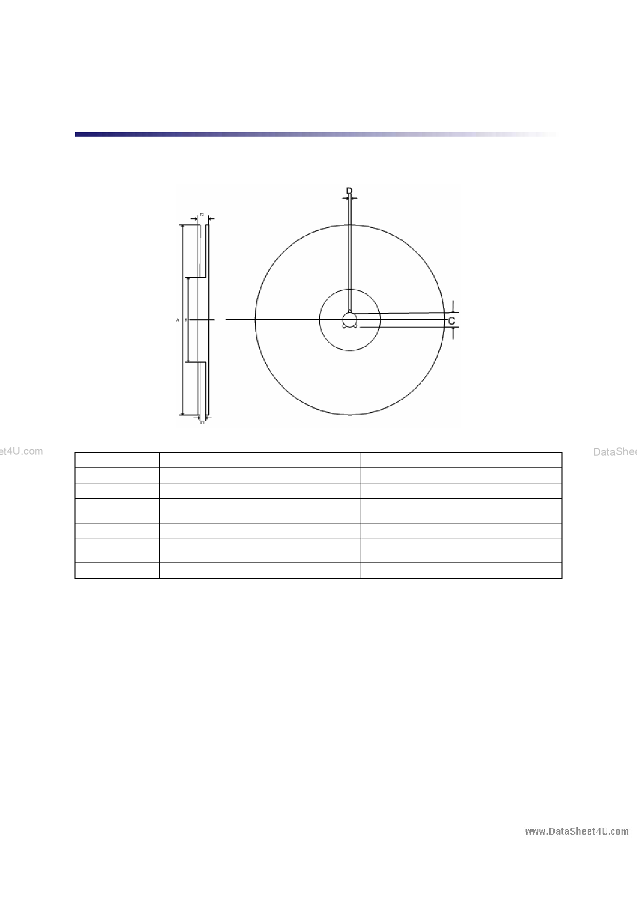
Product Tape and Reel Specifications
Reel Dimensions
PRELIMINARY
A
et4U.com
SOP 8PIN
Symbol
A
B
C
D
T1
T2
DataSheet4U.com
Description
Reel Outer Diameter
Reel Inner Diameter
Spindle Hole Diameter
Key Slit Width
Space Between Flange
Reel Thickness
Dimensions in mm
330±1.0
62±1.5
13.0+0.5
-0.2
2.0±0.15
12.8+0.3
-0.2
12.8±0.2
DataShee
DataSheet4U.com
DataSheet4 U .com
11 2004/4/26
11 Page | ||
| Páginas | Total 14 Páginas | |
| PDF Descargar | [ Datasheet L24W08.PDF ] | |
Hoja de datos destacado
| Número de pieza | Descripción | Fabricantes |
| L24W02 | Serial EEPROM | Link Smart |
| L24W04 | (L24W04 / L24W08) Serial EEPROM | Link Smart |
| L24W08 | (L24W04 / L24W08) Serial EEPROM | Link Smart |
| Número de pieza | Descripción | Fabricantes |
| SLA6805M | High Voltage 3 phase Motor Driver IC. |
Sanken |
| SDC1742 | 12- and 14-Bit Hybrid Synchro / Resolver-to-Digital Converters. |
Analog Devices |
|
DataSheet.es es una pagina web que funciona como un repositorio de manuales o hoja de datos de muchos de los productos más populares, |
| DataSheet.es | 2020 | Privacy Policy | Contacto | Buscar |
