|
|
|
PDF TNY277G Data sheet ( Hoja de datos )
| Número de pieza | TNY277G | |
| Descripción | (TNY274 - TNY280) Energy Efficient / Off-Line Switcher | |
| Fabricantes | Power Integrations | |
| Logotipo | ||
Hay una vista previa y un enlace de descarga de TNY277G (archivo pdf) en la parte inferior de esta página. Total 24 Páginas | ||
|
No Preview Available !
www.DataSheet4U.com
TNY274-280
TinySwitch®-III Family
Energy Efficient, Off-Line Switcher with
Enhanced Flexibility and Extended Power Range
Product Highlights
+
+
Lowest System Cost with Enhanced Flexibility
• Simple ON/OFF control, no loop compensation needed
• Selectable current limit through BP/M capacitor value
- Higher current limit extends peak power or, in open
frame applications, maximum continuous power
- Lower current limit improves efficiency in enclosed
adapters/chargers
- Allows optimum TinySwitch-III choice by swapping
devices with no other circuit redesign
Wide-Range
HV DC Input
D
TinySwitch-III
S
-
EN/UV
BP/M
DC
Output
-
PI-4095-082205
• Tight I2f parameter tolerance reduces system cost
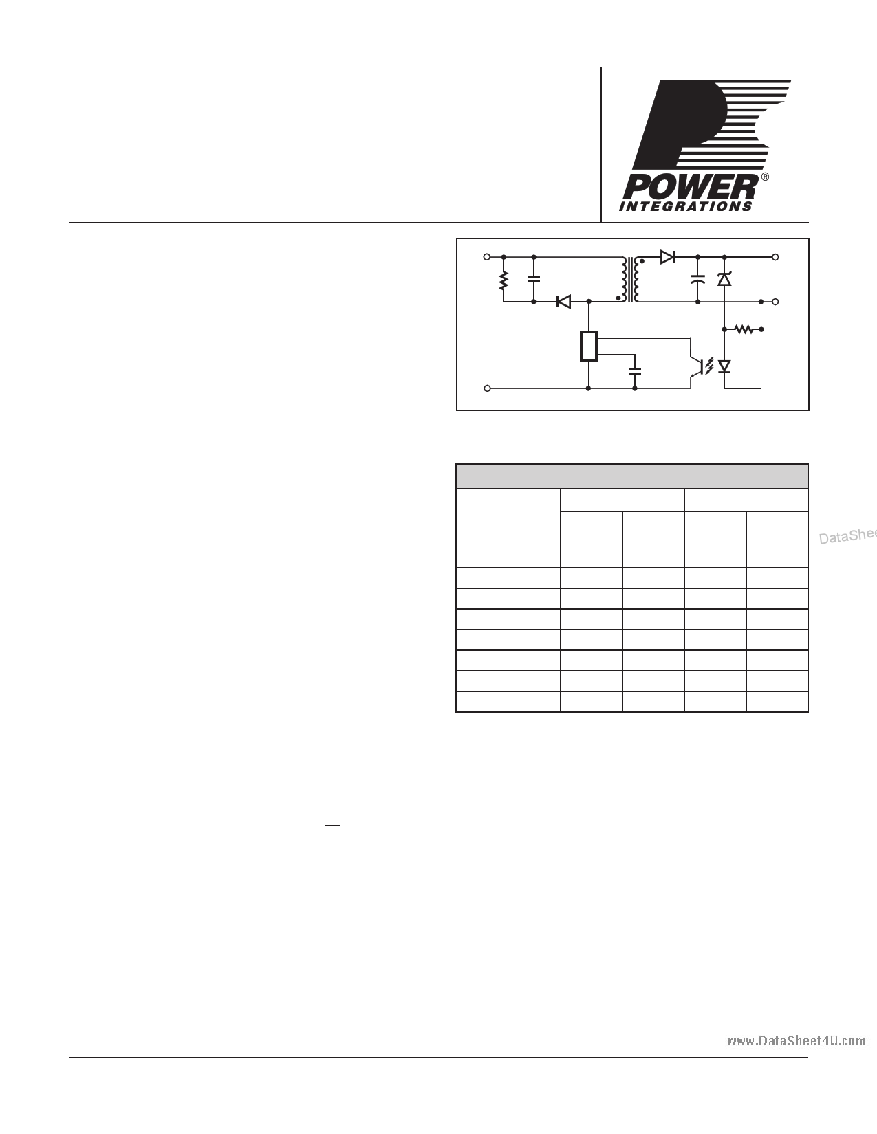
Figure 1. Typical Standby Application.
- Maximizes MOSFET and magnetics power delivery
- Minimizes max overload power, reducing cost of
transformer, primary clamp & secondary components
OUTPUT POWER TABLE
• ON-time extension – extends low line regulation range/
230 VAC ±15%
85-265 VAC
•
•
•
hold-up time to reduce input bulk capacitance
Self-biased: no bias winding or bias components
Frequency jittering reduces EMI filter costs
Pin-out simplifies heatsinking to the PCB
PRODUCT3
DataSheet4U.com
Peak or
Peak or
Adapter1 Open Adapter1 Open
Frame2
Frame2
DataShee
• SOURCE pins are electrically quiet for low EMI
TNY274 P or G 6 W 11 W 5 W 8.5 W
TNY275 P or G 8.5 W 15 W 6 W 11.5 W
Enhanced Safety and Reliability Features
• Accurate hysteretic thermal shutdown protection with
automatic recovery eliminates need for manual reset
TNY276 P or G 10 W 19 W
TNY277 P or G 13 W 23.5 W
7W
8W
15 W
18 W
• Improved auto-restart delivers <3% of maximum power
TNY278 P or G 16 W 28 W 10 W 21.5 W
in short circuit and open loop fault conditions
TNY279 P or G 18 W 32 W 12 W 25 W
• Output overvoltage shutdown with optional Zener
• Line under-voltage detect threshold set using a single
TNY280 P or G 20 W 36.5 W 14 W 28.5 W
optional resistor
• Very low component count enhances reliability and
enables single-sided printed circuit board layout
• High bandwidth provides fast turn on with no overshoot
and excellent transient load response
Table 1. Notes: 1. Minimum continuous power in a typical non-
ventilated enclosed adapter measured at 50 °C ambient. Use of an
external heatsink will increase power capability 2. Minimum peak
power capability in any design or minimum continuous power in an
open frame design (see Key Application Considerations). 3. Packages:
P: DIP-8C, G: SMD-8C. See Part Ordering Information.
• Extended creepage between DRAIN and all other pins
improves field reliability
EcoSmart®– Extremely Energy Efficient
• Easily meets all global energy efficiency regulations
• No-load <150 mW at 265 VAC without bias winding,
<50 mW with bias winding
• ON/OFF control provides constant efficiency down to
very light loads – ideal for mandatory CEC regulations
and 1 W PC standby requirements
Applications
• Chargers/adapters for cell/cordless phones, PDAs, digital
cameras, MP3/portable audio, shavers, etc.
DataSheet4U.com
• PC Standby and other auxiliary supplies
• DVD/PVR and other low power set top decoders
• Supplies for appliances, industrial systems, metering, etc.
Description
TinySwitch-III incorporates a 700 V power MOSFET, oscillator,
high voltage switched current source, current limit (user
selectable) and thermal shutdown circuitry. The IC family uses
an ON/OFF control scheme and offers a design flexible solution
with a low system cost and extended power capability.
February 2006
DataSheet4 U .com
DataSheet4U.com
1 page 
www.DataSheet4U.com
TNY274-280
load is proportional to the primary inductance of the transformer
and peak primary current squared. Hence, designing the supply
involves calculating the primary inductance of the transformer
for the maximum output power required. If the TinySwitch-III
is appropriately chosen for the power level, the current in the
calculated inductance will ramp up to current limit before the
DCMAX limit is reached.
Enable Function
TinySwitch-III senses the EN/UV pin to determine whether or
VEN
CLOCK
DCMAX
IDRAIN
not to proceed with the next switching cycle. The sequence of
cycles is used to determine the current limit. Once a cycle is
started, it always completes the cycle (even when the EN/UV
pin changes state half way through the cycle). This operation
results in a power supply in which the output voltage ripple
is determined by the output capacitor, amount of energy per
switch cycle and the delay of the feedback.
The EN/UV pin signal is generated on the secondary by
comparing the power supply output voltage with a reference
voltage. The EN/UV pin signal is high when the power supply
output voltage is less than the reference voltage.
In a typical implementation, the EN/UV pin is driven by an
optocoupler. The collector of the optocoupler transistor is
connected to the EN/UV pin and the emitter is connected to
the SOURCE pin. The optocoupler LED is connected in series
with a Zener diode across the DC output voltage to be regulated.
When the output voltage exceeds the target regulation voltage
level (optocoupler LED voltage drop plus Zener voltage), the
optocoupler LED will start to conduct, pulling the EN/UV pin
low. The Zener diode can be replaced by a TL431 reference
circuit for improved accuracy.
et4U.com
VDRAIN
Figure 6. Operation at Near Maximum Loading.
ON/OFF Operation with Current Limit State Machine
The internal clock of the TinySwitch-III runs all the time. At
the beginning of each clock cycle, it samples the EN/UV pin to
DataShee
DataSheet4dUe.cciodme whether or not to implement a switch cycle, and based
on the sequence of samples over multiple cycles, it determines
the appropriate current limit. At high loads, the state machine
PI-2749-082305
sets the current limit to its highest value. At lighter loads, the
state machine sets the current limit to reduced values.
VEN
CLOCK
DCMAX
VEN
CLOCK
DCMAX
IDRAIN
IDRAIN
VDRAIN
VDRAIN
DataSheet4FUigu.creom7. Operation at Moderately Heavy Loading.
PI-2667-082305
Figure 8. Operation at Medium Loading.
DataSheet4 U .com
DataSheet4U.com
PI-2377-082305
5E
2/06
5 Page 
www.DataSheet4U.com
TNY274-280
TOP VIEW
+
HV DC
INP-UT
Input Filter
Capacitor
CBP
S SSS
TinySwitch-III
CapYa1c-itor
T
r
a
n
s
f
o
r
m
e
r
Output Filter
Capacitor
et4U.com
EN/UV BP/M D
Opto-
coupler
DataSheet4U.com
Maximize hatched copper
areas (
) for optimum
heatsinking
-
DC
OUT
+
Figure 15. Recommended Circuit Board Layout for TinySwitch-III with Under-Voltage Lock Out Resistor.
DataShee
PI-4278-013006
Thermal Considerations
The four SOURCE pins are internally connected to the IC lead
frame and provide the main path to remove heat from the device.
Therefore all the SOURCE pins should be connected to a copper
area underneath the TinySwitch-III to act not only as a single
point ground, but also as a heatsink. As this area is connected
to the quiet source node, this area should be maximized for
good heatsinking. Similarly for axial output diodes, maximize
the PCB area connected to the cathode.
Y-Capacitor
The placement of the Y-capacitor should be directly from the
primary input filter capacitor positive terminal to the common/
return terminal of the transformer secondary. Such a placement
will route high magnitude common mode surge currents away
from the TinySwitch-III device. Note – if an input π (C, L, C)
EMI filter is used then the inductor in the filter should be placed
between the negative terminals of the input filter capacitors.
DataSheet4U.com
DataSheet4 U .com
Optocoupler
Place the optocoupler physically close to the TinySwitch-III
to minimizing the primary-side trace lengths. Keep the high
current, high voltage drain and clamp traces away from the
optocoupler to prevent noise pick up.
Output Diode
For best performance, the area of the loop connecting the
secondary winding, the output diode and the output filter
capacitor, should be minimized. In addition, sufficient copper
area should be provided at the anode and cathode terminals
of the diode for heatsinking. A larger area is preferred at the
quiet cathode terminal. A large anode area can increase high
frequency radiated EMI.
DataSheet4U.com
11E
2/06
11 Page | ||
| Páginas | Total 24 Páginas | |
| PDF Descargar | [ Datasheet TNY277G.PDF ] | |
Hoja de datos destacado
| Número de pieza | Descripción | Fabricantes |
| TNY277 | (TNY274 - TNY280) Energy Efficient / Off-Line Switcher | Power Integrations |
| TNY277G | (TNY274 - TNY280) Energy Efficient / Off-Line Switcher | Power Integrations |
| TNY277P | (TNY274 - TNY280) Energy Efficient / Off-Line Switcher | Power Integrations |
| Número de pieza | Descripción | Fabricantes |
| SLA6805M | High Voltage 3 phase Motor Driver IC. |
Sanken |
| SDC1742 | 12- and 14-Bit Hybrid Synchro / Resolver-to-Digital Converters. |
Analog Devices |
|
DataSheet.es es una pagina web que funciona como un repositorio de manuales o hoja de datos de muchos de los productos más populares, |
| DataSheet.es | 2020 | Privacy Policy | Contacto | Buscar |