|
|
PDF 103FA-5 Data sheet ( Hoja de datos )
| Número de pieza | 103FA-5 | |
| Descripción | REG103FA | |
| Fabricantes | Burr-Brown Corporation | |
| Logotipo |  |
|
Hay una vista previa y un enlace de descarga de 103FA-5 (archivo pdf) en la parte inferior de esta página. Total 13 Páginas | ||
|
No Preview Available !
®
For most current data sheet and other product
information, visit www.burr-brown.com
REG103
REG103
REG103
REG103
DMOS
500mA Low Dropout Regulator
FEATURES
q NEW DMOS TOPOLOGY:
Ultra Low Dropout Voltage:
115mV typ at 500mA and 3.3V Output
Output capacitor NOT required for stability
q FAST TRANSIENT RESPONSE
q VERY LOW NOISE: 33µVrms
q HIGH ACCURACY: ±2% max
q HIGH EFFICIENCY:
IGND = 1mA at IOUT = 500mA
Not Enabled: IGND = 0.5µA
q 2.5V, 2.7V, 3.0V, 3.3V, 5.0V AND
ADJUSTABLE OUTPUT VERSIONS
q FOLDBACK CURRENT LIMIT
q THERMAL PROTECTION
q OUTPUT VOLTAGE ERROR INDICATOR(1)
q SMALL SURFACE-MOUNT PACKAGES:
SOT223-5, DDPAK-5, SO-8
APPLICATIONS
q PORTABLE COMMUNICATION DEVICES
q BATTERY-POWERED EQUIPMENT
q PERSONAL DIGITAL ASSISTANTS
q MODEMS
q BAR-CODE SCANNERS
q BACKUP POWER SUPPLIES
DESCRIPTION
The REG103 is a family of low noise, low dropout
linear regulators with low ground pin current. Its new
DMOS topology provides significant improvement
over previous designs, including low dropout voltage
(only 115mV typ at full load), and better transient
performance. In addition, no output capacitor is re-
quired for stability, unlike conventional low dropout
regulators that are difficult to compensate and require
expensive low ESR capacitors greater than 1µF.
Typical ground pin current is only 1mA (at IOUT =
500mA) and drops to 0.5µA in “not enabled” mode.
Unlike regulators with PNP pass devices, quiescent
current remains relatively constant over load varia-
tions and under dropout conditions.
The REG103 has very low output noise (typically
33µVrms for VOUT = 3.3V with CNR = 0.01µF),
making it ideal for use in portable communications
equipment. On-chip trimming results in high output
voltage accuracy. Accuracy is maintained over tem-
perature, line, and load variations. Key parameters are
guaranteed over the specified temperature range
(–40°C to +85°C).
The SO-8 version of the REG103 has an Error pin
which provides a “power good” flag indicating the
regulator is in regulation. The REG103 is well pro-
tected: internal circuitry provides a current limit which
protects the load from damage. Thermal protection
circuitry keeps the chip from being damaged by exces-
sive temperature. In addition to the SO-8 package, the
REG103 is also available in the DDPAK and the
SOT223-5.
Enable Error(1)
Enable Error(1)
VIN
+
0.1µF
REG103
(Fixed Voltage
Versions)
NR Gnd
NR = Noise Reduction
VOUT
+ COUT(2)
VIN
+
0.1µF
NOTE: (1) SO-8 Package Only. (2) Optional.
REG103-A
Gnd
R1 +
Adj
VOUT
COUT(2)
R2
International Airport Industrial Park • Mailing Address: PO Box 11400, Tucson, AZ 85734 • Street Address: 6730 S. Tucson Blvd., Tucson, AZ 85706 • Tel: (520) 746-1111
Twx: 910-952-1111 • Internet: http://www.burr-brown.com/ • Cable: BBRCORP • Telex: 066-6491 • FAX: (520) 889-1510 • Immediate Product Info: (800) 548-6132
©2000 Burr-Brown Corporation
PDS-11527C
REPriGnte1d i0n U3.S.A. July, 2000
®
1 page 
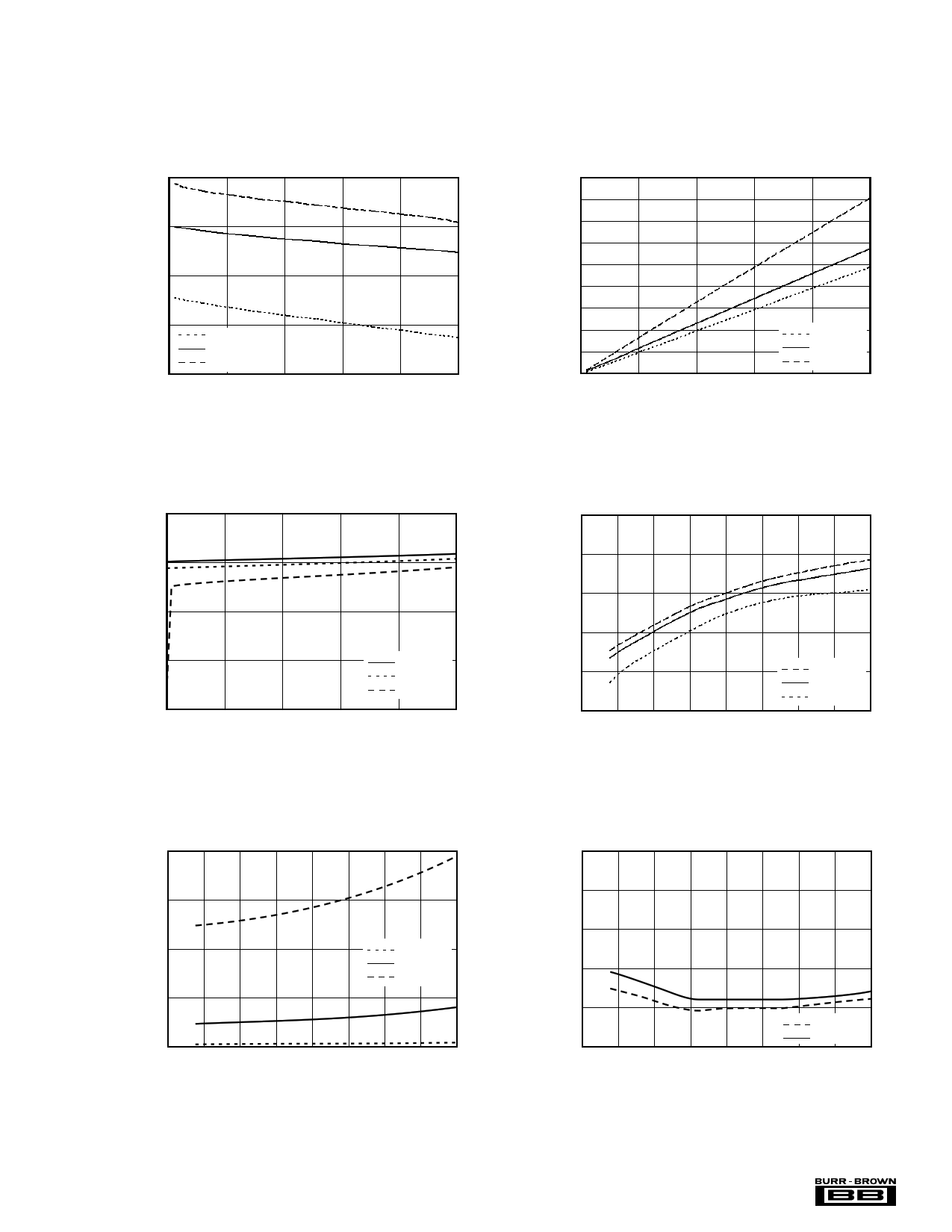
TYPICAL PERFORMANCE CURVES
For all models, at TJ = +25°C and VENABLE = 2V, unless otherwise noted.
OUTPUT VOLTAGE CHANGE vs IOUT
(VIN = VOUT + 1V, Output Voltage % Change
Refered to IOUT = 10mA at +25°C)
0.5
0
–0.5
–1.0
–1.5
0
= –55°C
= +25°C
= +125°C
100 200
300 400
500
IOUT (mA)
180
160
140
120
100
80
60
40
20
0
0
DC DROPOUT VOLTAGE vs OUTPUT CURRENT
= –55°C
= +25°C
= +125°C
100 200 300 400
Output Current (mA)
500
0.5
0
–0.5
–1.0
–1.5
0
OUTPUT VOLTAGE CHANGE vs VIN
(Output Voltage % Change Refered
to VIN = VOUT + 1V at IOUT = 10mA)
= 10mA
= 100mA
= 500mA
2 46 8
Input Voltage Above VOUT
10
OUTPUT VOLTAGE vs TEMPERATURE
(Output Voltage % Change Referred to
IOUT = 10mA at +25°C)
0.1
0.5
0
–0.5
–1
–1.5
–75 –50 –25
0 25 50
Temperature (°C)
= 10mA
= 100mA
= 500mA
75 100 125
DC DROPOUT VOLTAGE vs TEMPERATURE
160
120
80 = 10mA
= 100mA
= 500mA
40
0
–75 –50 –25
0 25 50
Temperature (°C)
75 100 125
LINE REGULATION vs TEMPERATURE
(VIN = VOUT + 1V to VIN = 15V )
0.5
0.4
0.3
0.2
0.1
0
–75 –50 –25
0 25 50
Temperature (°C)
= 10mA
= 100mA
75 100 125
®
5 REG103
5 Page 
NR
(fixed output
versions only)
CNR
(optional)
VREF
(1.295V)
Enable
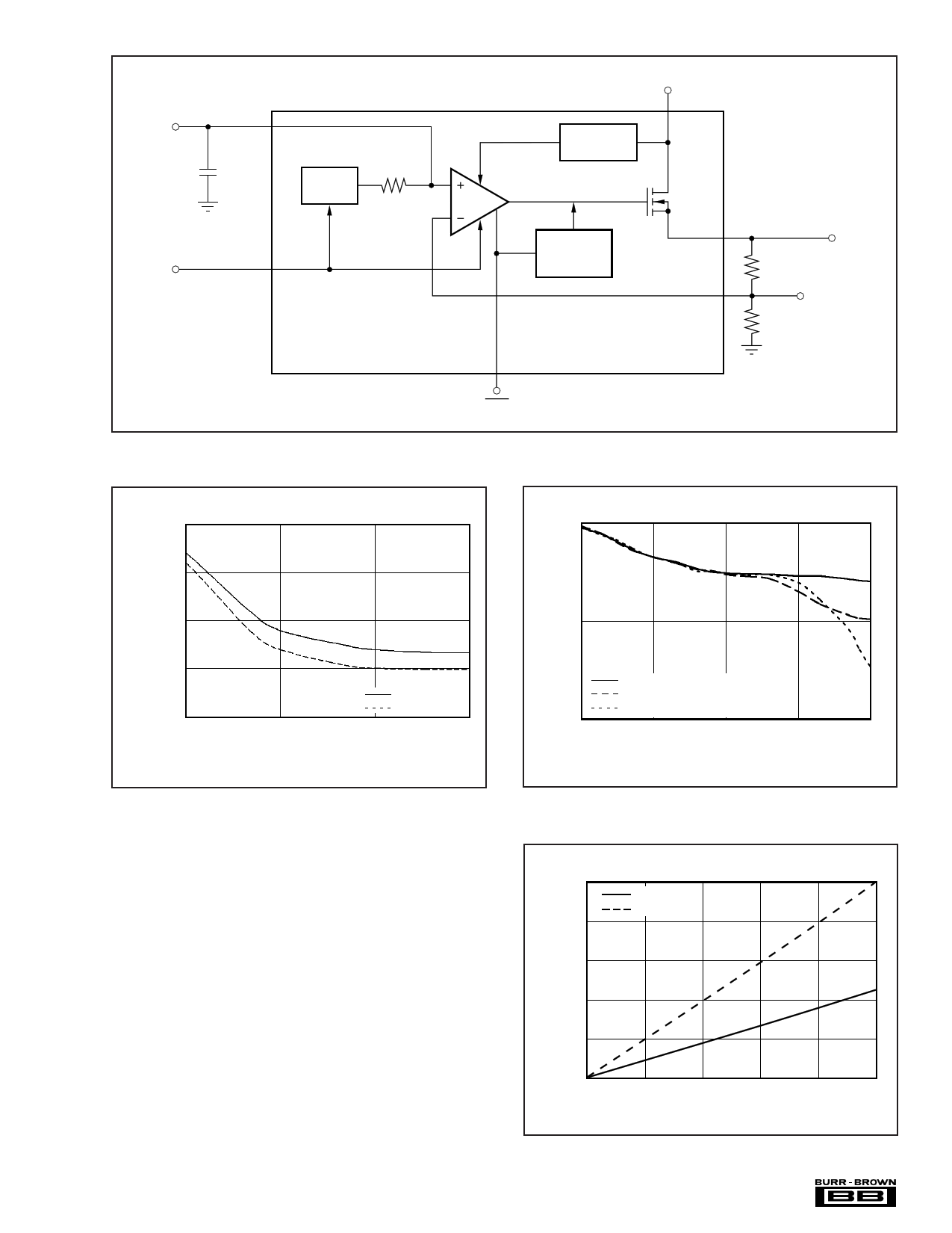
FIGURE 7. Block Diagram.
45
VIN
Low Noise
Charge Pump
Over Current
Over Temp
Protection
Error
DMOS
Output
VOUT
R1
Adj
(Adjustable
R2 Versions)
REG103
NOTE: R1 and R2 are internal
on fixed output versions.
10.0
35 1.0
25
0.001
0.01
CNR (µF)
COUT = 0
COUT = 10µF
0.1 1
0.1
10
COUT = 0, CFB = 0
COUT = 0, CFB = 0.01µF
COUT = 10µF, CFB = 0.01µF
100 1000
Frequency
10000
100000
FIGURE 8. Output Noise versus Noise Reduction Capacitor. FIGURE 9. Output Noise Density on Adjustable Versions.
regulator’s input-to-output resistance is the RdsON of the
DMOS pass element (typically 230mΩ). For static (DC)
loads, the REG103 will typically maintain regulation down
to VIN to VOUT voltage drop of 115mV at full rated output
current. In Figure 10, the bottom line (DC dropout) shows
the minimum VIN to VOUT voltage drop required to prevent
drop-out under DC load conditions.
For large step changes in load current, the REG103 requires
a larger voltage drop across it to avoid degraded transient
response. The boundary of this “transient drop-out” region is
shown as the top line in Figure 10. Values of VIN to VOUT
voltage drop above this line insure normal transient re-
sponse.
In the transient dropout region between “DC” and “Tran-
sient”, transient response recovery time increases. The time
required to recover from a load transient is a function of both
the magnitude and rate of the step change in load current and
REG103 –3.3 at 25°C
250
DC
Transient
200
150
100
50
0
0 100 200 300 400
IOUT (mA)
FIGURE 10. Transient and DC Dropout.
11 REG103
500
®
11 Page | ||
| Páginas | Total 13 Páginas | |
| PDF Descargar | [ Datasheet 103FA-5.PDF ] | |
Hoja de datos destacado
| Número de pieza | Descripción | Fabricantes |
| 103FA-5 | REG103FA | Burr-Brown Corporation |
| Número de pieza | Descripción | Fabricantes |
| SLA6805M | High Voltage 3 phase Motor Driver IC. |
Sanken |
| SDC1742 | 12- and 14-Bit Hybrid Synchro / Resolver-to-Digital Converters. |
Analog Devices |
|
DataSheet.es es una pagina web que funciona como un repositorio de manuales o hoja de datos de muchos de los productos más populares, |
| DataSheet.es | 2020 | Privacy Policy | Contacto | Buscar |
