|
|
PDF LM3224 Data sheet ( Hoja de datos )
| Número de pieza | LM3224 | |
| Descripción | 615kHz/1.25MHz Step-up PWM DC/DC Converter | |
| Fabricantes | National Semiconductor | |
| Logotipo | ||
Hay una vista previa y un enlace de descarga de LM3224 (archivo pdf) en la parte inferior de esta página. Total 18 Páginas | ||
|
No Preview Available !
www.DataSheet4U.com
December 2004
LM3224
615kHz/1.25MHz Step-up PWM DC/DC Converter
General Description
The LM3224 is a step-up DC/DC converter with a 0.15Ω
(typ.), 2.45A (typ.) internal switch and pin selectable operat-
ing frequency. With the ability to convert 3.3V to multiple
outputs of 8V, -8V, and 23V, the LM3224 is an ideal part for
biasing TFT displays. With the high current switch it is also
ideal for driving high current white LEDs for flash applica-
tions. The LM3224 can be operated at switching frequencies
of 615kHz and 1.25MHz allowing for easy filtering and low
noise. An external compensation pin gives the user flexibility
in setting frequency compensation, which makes possible
the use of small, low ESR ceramic capacitors at the output.
An external soft-start pin allows the user to control the
amount of inrush current during start up. The LM3224 is
available in a low profile 8-lead MSOP package.
Features
n Operating voltage range of 2.7V to 7V
n 615kHz/1.25MHz pin selectable frequency operation
n Over temperature protection
n Optional soft-start function
n 8-Lead MSOP package
Applications
n TFT Bias Supplies
n Handheld Devices
n Portable Applications
n GSM/CDMA Phones
n Digital Cameras
n White LED Flash/Torch Applications
Typical Application Circuit
www.DataSheet4U.com
© 2004 National Semiconductor Corporation DS200976
20097631
www.national.com
www.DataSheet4U.com
1 page 
www.DataSheet4U.com
Electrical Characteristics (Continued)
Note 5: The human body model is a 100 pF capacitor discharged through a 1.5kΩ resistor into each pin. The machine model is a 200pF capacitor discharged
directly into each pin.
Note 6: All limits guaranteed at room temperature (standard typeface) and at temperature extremes (bold typeface). All room temperature limits are 100%
production tested. All limits at temperature extremes are guaranteed via correlation using standard Statistical Quality Control (SQC) methods. All limits are used to
calculate Average Outgoing Quality Level (AOQL).
Note 7: Typical numbers are at 25˚C and represent the most likely norm.
Note 8: Duty cycle affects current limit due to ramp generator.
Note 9: Current limit at 0% duty cycle. See TYPICAL PERFORMANCE section for Switch Current Limit vs. VIN
Note 10: Bias current flows into FB pin.
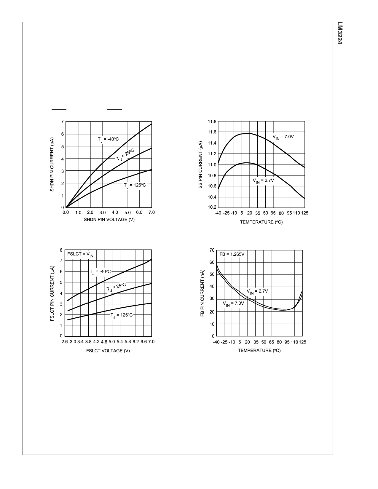
Typical Performance Characteristics
SHDN Pin Current vs. SHDN Pin Voltage
SS Pin Current vs. Temperature
20097616
20097617
www.DataSheet4U.comFSLCT Pin Current vs. FSLCT Pin Voltage
FB Pin Current vs. Temperature
20097618
5
20097619
www.national.com
www.DataSheet4U.com
5 Page 
www.DataSheet4U.com
Operation (Continued)
must exceed the switch current limit. Using Schottky diodes
with lower forward voltage drop will decrease power dissipa-
tion and increase efficiency.
DC GAIN AND OPEN-LOOP GAIN
Since the control stage of the converter forms a complete
feedback loop with the power components, it forms a closed-
loop system that must be stabilized to avoid positive feed-
back and instability. A value for open-loop DC gain will be
required, from which you can calculate, or place, poles and
zeros to determine the crossover frequency and the phase
margin. A high phase margin (greater than 45˚) is desired for
the best stability and transient response. For the purpose of
stabilizing the LM3224, choosing a crossover point well be-
low where the right half plane zero is located will ensure
sufficient phase margin.
To ensure a bandwidth of 1⁄2 or less of the frequency of the
RHP zero, calculate the open-loop DC gain, ADC. After this
value is known, you can calculate the crossover visually by
placing a −20dB/decade slope at each pole, and a +20dB/
decade slope for each zero. The point at which the gain plot
crosses unity gain, or 0dB, is the crossover frequency. If the
crossover frequency is less than 1⁄2 the RHP zero, the phase
margin should be high enough for stability. The phase mar-
gin can also be improved by adding CC2 as discussed later in
this section. The equation for ADC is given below with addi-
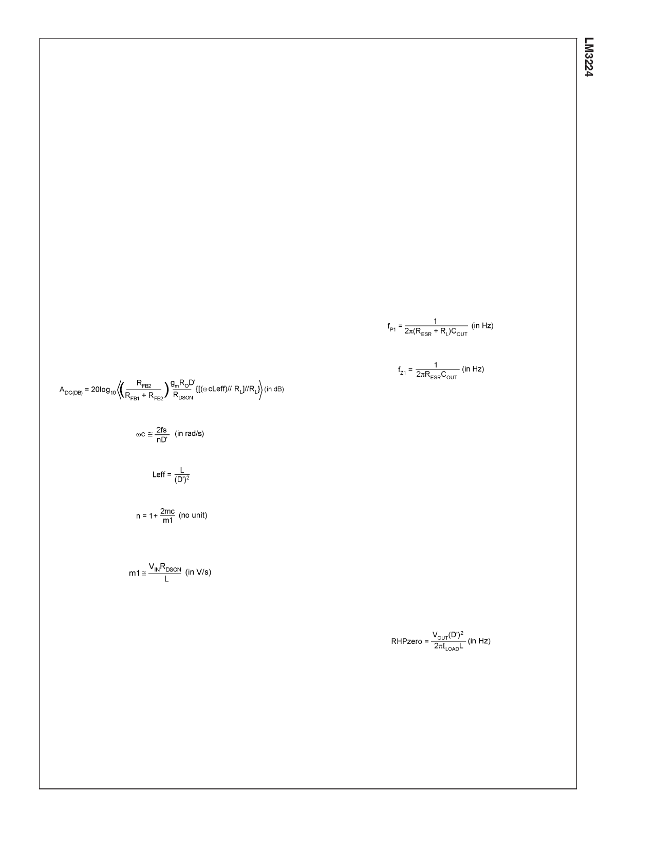
tional equations required for the calculation:
source output. The size will generally need to be larger for
applications where the regulator is supplying nearly the
maximum rated output or if large load steps are expected. A
minimum value of 10µF should be used for the less stressful
condtions while a 22µF to 47µF capacitor may be required
for higher power and dynamic loads. Larger values and/or
lower ESR may be needed if the application requires very
low ripple on the input source voltage.
The choice of output capacitors is also somewhat arbitrary
and depends on the design requirements for output voltage
ripple. It is recommended that low ESR (Equivalent Series
Resistance, denoted RESR) capacitors be used such as
ceramic, polymer electrolytic, or low ESR tantalum. Higher
ESR capacitors may be used but will require more compen-
sation which will be explained later on in the section. The
ESR is also important because it determines the peak to
peak output voltage ripple according to the approximate
equation:
∆VOUT ) 2∆iLRESR (in Volts)
A minimum value of 10µF is recommended and may be
increased to a larger value. After choosing the output capaci-
tor you can determine a pole-zero pair introduced into the
control loop by the following equations:
Where RL is the minimum load resistance corresponding to
www.DataSheet4U.comthe maximum load current. The zero created by the ESR of
the output capacitor is generally very high frequency if the
ESR is small. If low ESR capacitors are used it can be
neglected. If higher ESR capacitors are used see the High
Output Capacitor ESR Compensation section. Some suit-
able capacitor vendors include Vishay, Taiyo-Yuden, and
TDK.
mc ) 0.072fs (in V/s)
where RL is the minimum load resistance, VIN is the mini-
mum input voltage, gm is the error amplifier transconduc-
tance found in the Electrical Characteristics table, and RD-
SON is the value chosen from the graph "NMOS RDSON vs.
Input Voltage" in the Typical Performance Characteristics
section.
INPUT AND OUTPUT CAPACITOR SELECTION
The switching action of a boost regulator causes a triangular
voltage waveform at the input. A capacitor is required to
reduce the input ripple and noise for proper operation of the
regulator. The size used is dependant on the application and
board layout. If the regulator will be loaded uniformly, with
very little load changes, and at lower current outputs, the
input capacitor size can often be reduced. The size can also
be reduced if the input of the regulator is very close to the
RIGHT HALF PLANE ZERO
A current mode control boost regulator has an inherent right
half plane zero (RHP zero). This zero has the effect of a zero
in the gain plot, causing an imposed +20dB/decade on the
rolloff, but has the effect of a pole in the phase, subtracting
another 90˚ in the phase plot. This can cause undesirable
effects if the control loop is influenced by this zero. To ensure
the RHP zero does not cause instability issues, the control
loop should be designed to have a bandwidth of less than 1⁄2
the frequency of the RHP zero. This zero occurs at a fre-
quency of:
where ILOAD is the maximum load current.
SELECTING THE COMPENSATION COMPONENTS
The first step in selecting the compensation components RC
and CC is to set a dominant low frequency pole in the control
loop. Simply choose values for RC and CC within the ranges
given in the Introduction to Compensation section to set this
pole in the area of 10Hz to 500Hz. The frequency of the pole
created is determined by the equation:
11 www.national.com
www.DataSheet4U.com
11 Page | ||
| Páginas | Total 18 Páginas | |
| PDF Descargar | [ Datasheet LM3224.PDF ] | |
Hoja de datos destacado
| Número de pieza | Descripción | Fabricantes |
| LM322 | Precision Timers | National Semiconductor |
| LM3224 | LM3224 615kHz/1.25MHz Step-up PWM DC/DC Converter (Rev. C) | Texas Instruments |
| LM3224 | 615kHz/1.25MHz Step-up PWM DC/DC Converter | National Semiconductor |
| Número de pieza | Descripción | Fabricantes |
| SLA6805M | High Voltage 3 phase Motor Driver IC. |
Sanken |
| SDC1742 | 12- and 14-Bit Hybrid Synchro / Resolver-to-Digital Converters. |
Analog Devices |
|
DataSheet.es es una pagina web que funciona como un repositorio de manuales o hoja de datos de muchos de los productos más populares, |
| DataSheet.es | 2020 | Privacy Policy | Contacto | Buscar |
