|
|
|
PDF TOP245 Data sheet ( Hoja de datos )
| Número de pieza | TOP245 | |
| Descripción | (TOP242 - TOP250) up to 290 W Extended Power / Integrated Off-line Switcher Family | |
| Fabricantes | Power Integrations | |
| Logotipo | ||
Hay una vista previa y un enlace de descarga de TOP245 (archivo pdf) en la parte inferior de esta página. Total 30 Páginas | ||
|
No Preview Available !
www.DataSheet4U.com
TOP242-250
TOPSwitch®-GX Family
Extended Power, Design Flexible,
EcoSmart,® Integrated Off-line Switcher
Product Highlights
Lower System Cost, High Design Flexibility
• Extended power range for higher power applications
• No heatsink required up to 30 W using P package
• Features eliminate or reduce cost of external components
• Fully integrated soft-start for minimum stress/overshoot
• Externally programmable accurate current limit
• Wider duty cycle for more power, smaller input capacitor
• Separate line sense and current limit pins on Y/R/F packages
• Line under-voltage (UV) detection: no turn off glitches
• Line overvoltage (OV) shutdown extends line surge limit
• Line feed forward with maximum duty cycle (DCMAX)
reduction rejects line ripple and limits DCMAX at high line
• Frequency jittering reduces EMI and EMI filtering costs
• Regulates to zero load without dummy loading
• 132 kHz frequency reduces transformer/power supply size
• Half frequency option in Y/R/F packages for video applications
• Hysteretic thermal shutdown for automatic fault recovery
• Large thermal hysteresis prevents PC board overheating
EcoSmart - Energy Efficient
• Extremely low consumption in remote off mode
(80 mW @ 110 VAC, 160 mW @ 230 VAC)
• Frequency lowered with load for high standby efficiency
• Allows shutdown/wake-up via LAN/input port
Description
TOPSwitch-GX uses the same proven topology as TOPSwitch, cost
effectively integrating the high voltage power MOSFET, PWM
control, fault protection and other control circuitry onto a single
CMOS chip. Many new functions are integrated to
reduce system cost and improve design flexibility, performance
and energy efficiency.
Depending on package type, either 1 or 3 additional pins over the
TOPSwitch standard DRAIN, SOURCE and CONTROL terminals
allow the following functions: line sensing (OV/UV, line feed-
forward/DCMAX reduction), accurate externally set current limit,
remote ON/OFF, synchronization to an external lower frequency,
and frequency selection (132 kHz/66 kHz).
All package types provide the following transparent features: Soft-
start, 132 kHz switching frequency (automatically reduced at light
load), frequency jittering for lower EMI, wider DCMAX, hysteretic
tchriewtrimcwaallwpsah.rDuamtdaeottwearnsSa(ihn.ede. lceaurtrgr4eerUntc.rliecmeopitam,gferepqauceknacgye, sP.WInMadgdaiitnio)nh,aavlel
tighter temperature and absolute tolerance, to simplify design and
optimize system cost.
+
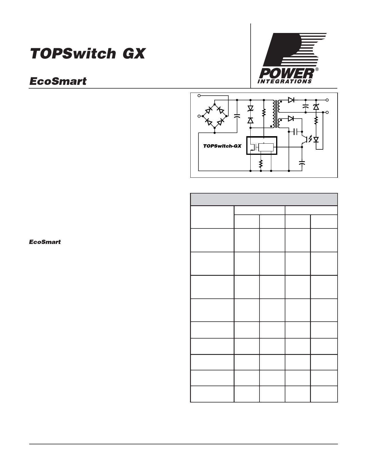
AC DC
IN OUT
-
DL
TOPSwitch-GX
CONTROL
C
S XF
Figure 1. Typical Flyback Application.
PI-2632-060200
OUTPUT POWER TABLE
PRODUCT3
230 VAC ±15%4
85-265 VAC
Adapter1
Open
Frame2
Adapter1
Open
Frame2
TOP242 P or G 9 W
TOP242 R 21 W
TOP242 Y or F 10 W
15 W
22 W
22 W
6.5 W
11 W
7W
10 W
14 W
14 W
TOP243 P or G 13 W
TOP243 R 29 W
TOP243 Y or F 20 W
25 W
45 W
45 W
9W
17 W
15 W
15 W
23 W
30 W
TOP244 P or G 16 W
TOP244 R 34 W
TOP244 Y or F 30 W
28 W
50 W
65 W
11 W
20 W
20 W
20 W
28 W
45 W
TOP245 P 19 W
TOP245 R 37 W
TOP245 Y or F 40 W
30 W
57 W
85 W
13 W
23 W
26 W
22 W
33 W
60 W
TOP246 R 40 W 64 W 26 W 38 W
TOP246 Y or F 60 W 125 W 40 W 90 W
TOP247 R 42 W 70 W 28 W 43 W
TOP247 Y or F 85 W 165 W 55 W 125 W
TOP248 R 43 W 75 W 30 W 48 W
TOP248 Y or F 105 W 205 W 70 W 155 W
TOP249 R 44 W 79 W 31 W 53 W
TOP249 Y or F 120 W 250 W 80 W 180 W
TOP250 R 45 W 82 W 32 W 55 W
TOP250 Y or F 135 W 290 W 90 W 210 W
Table 1. Notes: 1. Typical continuous power in a non-ventilated
enclosed adapter measured at 50 °C ambient. 2. Maximum practical
continuous power in an open frame design at 50 °C ambient. See
Key Applications for detailed conditions. 3. See Part Ordering
Information. 4. 230 VAC or 100/115 VAC with doubler.
September 2003
1 page 
www.DataSheet4U.com
TOP242-250
TOPSwitch-GX Family Functional Description
Like TOPSwitch, TOPSwitch-GX is an integrated switched
mode power supply chip that converts a current at the control
input to a duty cycle at the open drain output of a high voltage
power MOSFET. During normal operation the duty cycle of
the power MOSFET decreases linearly with increasing
CONTROL pin current as shown in Figure 7.
In addition to the three terminal TOPSwitch features, such as
the high voltage start-up, the cycle-by-cycle current limiting,
loop compensation circuitry, auto-restart, thermal shutdown,
the TOPSwitch-GX incorporates many additional functions that
reduce system cost, increase power supply performance and
design flexibility. A patented high voltage CMOS technology
allows both the high voltage power MOSFET and all the low
voltage control circuitry to be cost effectively integrated onto
a single monolithic chip.
Three terminals, FREQUENCY, LINE-SENSE, and
EXTERNAL CURRENT LIMIT (available in Y, R or F
package) or one terminal MULTI-FUNCTION (available in P
or G package) have been added to implement some of the new
functions. These terminals can be connected to the SOURCE
pin to operate the TOPSwitch-GX in a TOPSwitch-like three
terminal mode. However, even in this three terminal mode, the
TOPSwitch-GX offers many new transparent features that do
not require any external components:
1. A fully integrated 10 ms soft-start limits peak currents and
voltages during start-up and dramatically reduces or
eliminates output overshoot in most applications.
2. DC of 78% allows smaller input storage capacitor, lower
MAX
input voltage requirement and/or higher power capability.
3. Frequency reduction at light loads lowers the switching
losses and maintains good cross regulation in multiple
output supplies.
4. Higher switching frequency of 132 kHz reduces the
transformer size with no noticeable impact on EMI.
5. Frequency jittering reduces EMI.
6. Hysteretic over-temperature shutdown ensures automatic
recovery from thermal fault. Large hysteresis prevents circuit
board overheating.
7. Packages with omitted pins and lead forming provide large
drain creepage distance.
8. Tighter absolute tolerances and smaller temperature vari-
ations on switching frequency, current limit and PWM gain.
The LINE-SENSE (L) pin is usually used for line sensing by
connecting a resistor from this pin to the rectified DC high
voltage bus to implement line overvoltage (OV), under-voltage
(UV)
and
line
feed-forward
with
DC
MAX
reduction.
In this
mowdew, twhe.vDalauetaofSthheereesits4toUr d.ecteormmines the OV/UV thresholds
and the DC is reduced linearly starting from a line voltage
MAX
above the under-voltage threshold. See Table 2 and Figure 11.
Auto-restart
ICD1
132
IB
IL = 190 µA
IL = 125 µA
IL < IL(DC)
30
Auto-restart
ICD1
78
IC (mA)
IB
Slope = PWM Gain
38 IL = 125 µA
10 IL = 190 µA
IL < IL(DC)
TOP242-5 1.6 2.0
5.2 6.0
TOP246-9 2.2 2.6
5.8 6.6
TOP250 2.4 2.7
IC (mA)
6.5 7.3
Note: For P and G packages IL is replaced with IM.
PI-2633-011502
Figure 7. Relationship of Duty Cycle and Frequency to CONTROL
Pin Current.
The pin can also be used as a remote ON/OFF and a
synchronization input.
The EXTERNAL CURRENT LIMIT (X) pin is usually used to
reduce the current limit externally to a value close to the operating
peak current, by connecting the pin to SOURCE through a resistor.
This pin can also be used as a remote ON/OFF and a
synchronization input in both modes. See Table 2 and Figure 11.
For the P or G packages the LINE-SENSE and EXTERNAL
CURRENT LIMIT pin functions are combined on one MULTI-
FUNCTION (M) pin. However, some of the functions become
mutually exclusive as shown in Table 3.
The FREQUENCY (F) pin in the Y, R or F package sets the
switching frequency to the default value of 132 kHz when
connected to SOURCE pin. A half frequency option of 66 kHz
can be chosen by connecting this pin to CONTROL pin
instead. Leaving this pin open is not recommended.
5K
9/03
5 Page 
www.DataSheet4U.com
with
30
µA
hysteresis)
and
OV
triggers
at
I
OV
(+225
µA
typical with 8 µA hysteresis). Between the UV and OV
thresholds, the output is enabled. For line feed-forward with
DC reduction, the vertical axis represents the magnitude of
MAX
the DCMAX. Line feed-forward with DCMAX reduction lowers
maximum duty cycle from 78% at IL(DC) (+60 µA typical) to
38% at IOV (+225 µA).
EXTERNAL CURRENT LIMIT (X) Pin Operation
(Y, R and F Packages)
When current is drawn out of the EXTERNAL CURRENT
LIMIT pin, it works as a voltage source of approximately
1.3 V up to a maximum current of -240 µA (typical). At
-240 µA, it turns into a constant current source (refer to
Figure 12a).
There are two functions available through the use of the
EXTERNAL CURRENT LIMIT pin: external current limit
and remote ON/OFF. Connecting the EXTERNAL CURRENT
LIMIT pin and SOURCE pin disables the two functions. In
high efficiency applications this pin can be used to reduce the
current limit externally to a value close to the operating peak
current, by connecting the pin to the SOURCE pin through a
resistor. The pin can also be used for remote ON/OFF. Table 2
shows several possible combinations using this pin. See
Figure 11 for a description of the functions where the horizontal
axis (left hand side) represents the EXTERNAL CURRENT
LIMIT pin current. The meaning of the vertical axes varies
with function. For those that control the ON/OFF states of the
output such as remote ON/OFF, the vertical axis represents the
enable/disable states of the output. For external current limit,
the vertical axis represents the magnitude of the ILIMIT. Please
see graphs in the Typical Performance Characteristics section
for the current limit programming range and the selection of
appropriate resistor value.
TOP242-250
MULTI-FUNCTION (M) Pin Operation (P and G Packages)
The LINE-SENSE and EXTERNAL CURRENT LIMIT pin
functions are combined to a single MULTI-FUNCTION pin
for P and G packages. The comparator with a 1 V threshold at
the LINE-SENSE pin is removed in this case as shown in Figure
2b. All of the other functions are kept intact. However, since
some of the functions require opposite polarity of input current
(MULTI-FUNCTION pin), they are mutually exclusive. For
example, line sensing features cannot be used simultaneously
with external current limit setting. When current is fed into
the MULTI-FUNCTION pin, it works as a voltage source of
approximately 2.6 V up to a maximum current of +400 µA
(typical). At +400 µA, this pin turns into a constant current
sink. When current is drawn out of the MULTI-FUNCTION
pin, it works as a voltage source of approximately 1.3 V up to
a maximum current of -240 µA (typical). At -240 µA, it turns
into a constant current source. Refer to Figure 12b.
There are a total of five functions available through the use of
the MULTI-FUNCTION pin: OV, UV, line feed-forward with
DCMAX reduction, external current limit and remote ON/OFF.
A short circuit between the MULTI-FUNCTION pin and
SOURCE pin disables all five functions and forces
TOPSwitch-GX to operate in a simple three terminal mode like
TOPSwitch-II. The MULTI-FUNCTION pin is typically used
for line sensing by connecting a resistor from this pin to the
rectified DC high voltage bus to implement OV, UV and DCMAX
reduction with line voltage. In this mode, the value of the
resistor determines the line OV/UV thresholds, and the DCMAX
is reduced linearly with increasing rectified DC high voltage
starting from just above the UV threshold. External current
limit programming is implemented by connecting the MULTI-
FUNCTION pin to the SOURCE pin through a resistor.
However, this function is not necessary in most applications
since the internal current limit of the P and G package devices
has been reduced, compared to the Y, R and F package devices,
to match the thermal dissipation capability of the P and G
MULTI-FUNCTION PIN TABLE*
Figure Number
30 31 32 33 34 35
Three Terminal Operation
Under-Voltage
✔
✔✔
Overvoltage
✔✔
Line Feed-Forward (DCMAX)
Overload Power Limiting
✔
✔
External Current Limit
✔✔
Remote ON/OFF
*wThwis twab.leDisaotnalySa hpaerteialtl4istUof.mcoanmy MULTI-FUNCTION pin configurations that are possible.
Table 3. Typical MULTI-FUNCTION Pin Configurations.
36
✔
37 38
✔
✔✔
39 40
✔
✔
✔
✔
✔✔
11K
9/03
11 Page | ||
| Páginas | Total 30 Páginas | |
| PDF Descargar | [ Datasheet TOP245.PDF ] | |
Hoja de datos destacado
| Número de pieza | Descripción | Fabricantes |
| TOP242 | (TOP242 - TOP250) up to 290 W Extended Power / Integrated Off-line Switcher Family | Power Integrations |
| TOP242F | (TOP242 - TOP250) Family Extended Power/ Design Flexible/Integrated Off-line Switcher | Power Integrations |
| TOP242G | (TOP242 - TOP250) Family Extended Power/ Design Flexible/Integrated Off-line Switcher | Power Integrations |
| TOP242P | (TOP242 - TOP250) Family Extended Power/ Design Flexible/Integrated Off-line Switcher | Power Integrations |
| Número de pieza | Descripción | Fabricantes |
| SLA6805M | High Voltage 3 phase Motor Driver IC. |
Sanken |
| SDC1742 | 12- and 14-Bit Hybrid Synchro / Resolver-to-Digital Converters. |
Analog Devices |
|
DataSheet.es es una pagina web que funciona como un repositorio de manuales o hoja de datos de muchos de los productos más populares, |
| DataSheet.es | 2020 | Privacy Policy | Contacto | Buscar |