|
|
|
PDF ICS94201 Data sheet ( Hoja de datos )
| Número de pieza | ICS94201 | |
| Descripción | Programmable System Frequency Generator | |
| Fabricantes | Integrated Circuit Systems | |
| Logotipo | ||
Hay una vista previa y un enlace de descarga de ICS94201 (archivo pdf) en la parte inferior de esta página. Total 18 Páginas | ||
|
No Preview Available !
www.DataSheet4U.com
Integrated
Circuit
Systems, Inc.
ICS94201
Programmable System Frequency Generator for PII/III™
Recommended Application:
810/810E and Solano (815) type chipset
Output Features:
• 2 - CPUs @ 2.5V
• 13 - SDRAM @ 3.3V
• 3 - 3V66 @ 3.3V
• 8 - PCI @3.3V
• 1 - 24/48MHz@ 3.3V
• 1 - 48MHz @ 3.3V fixed
• 1 - REF @3.3V, 14.318MHz
Features:
• Programmable ouput frequency.
• Programmable ouput rise/fall time for PCI
and SDRAM clocks.
• Programmable 3V66 to PCI skew.
• Spread spectrum for EMI control
with programmable spread percentage.
• Watchdog timer technology to reset system
if over-clocking causes malfunction.
• Support power management through PD#.
• Uses external 14.318MHz crystal.
• FS pins for frequency select
Key Specifications:
• CPU Output Jitter: <250ps
• IOAPIC Output Jitter: <500ps
• 48MHz, 3V66, PCI Output Jitter: <500ps
• CPU Output Skew: <175ps
• PCI Output Skew: <500ps
• 3V66 Output Skew <175ps
• For group skew timing, please refer to the
Group Timing Relationship Table.
www.DataSheet4U.com
Pin Configuration
VDDREF
X1
X2
GNDREF
GND3V66
3V66-0
3V66-1
3V66-2
VDD3V66
VDDPCI
1*(FS0)PCICLK0
1*(FS1)PCICLK1
1*(SEL24_48#)PCICLK2
GNDPCI
PCICLK3
PCICLK4
PCICLK5
VDDPCI
PCICLK6
PCICLK7
GNDPCI
PD#
SCLK
SDATA
VDDSDR
SDRAM11
SDRAM10
GNDSDR
1
2
3
4
5
6
7
8
9
10
11
12
13
14
15
16
17
18
19
20
21
22
23
24
25
26
27
28
56 REF0(FS4)*1
55 VDDLAPIC
54 IOAPIC
53 VDDLCPU
52 CPUCLK0
51 CPUCLK1
50 GNDLCPU
49 GNDSDR
48 SDRAM0
47 SDRAM1
46 SDRAM2
45 VDDSDR
44 SDRAM3
43 SDRAM4
42 SDRAM5
41 GNDSDR
40 SDRAM6
39 SDRAM7
38 SDRAM_F
37 VDDSDR
36 GND48
35 24_48MHz(FS2)*
34 48MHz(FS3)*1
33 VDD48
32 VDDSDR
31 SDRAM8
30 SDRAM9
29 GNDSDR
56-Pin 300 mil SSOP
1. These pins will have 1.5 to 2X drive strength.
* 120K ohm pull-up to VDD on indicated inputs.
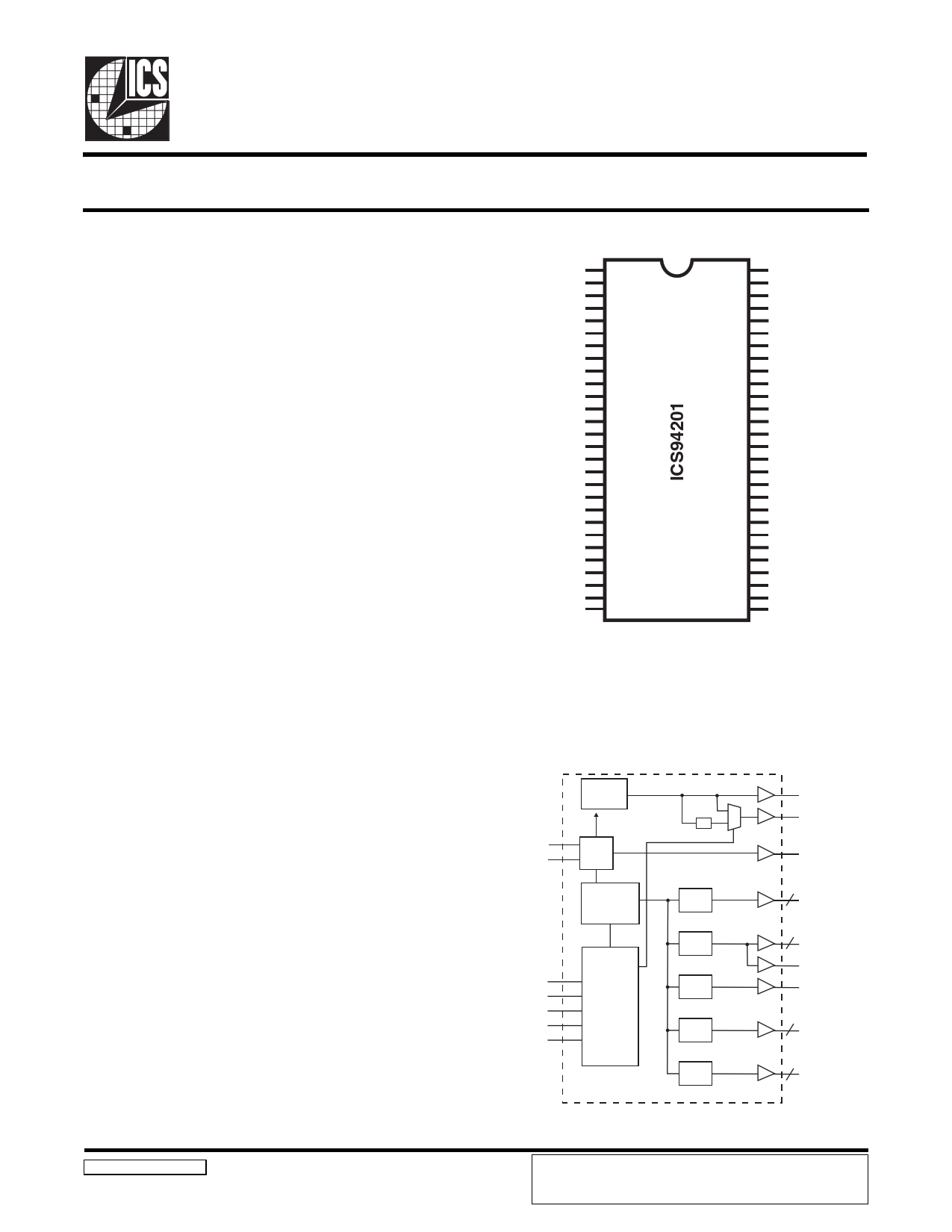
Block Diagram
PLL2
X1 XTAL
X2 OSC
PLL1
Spread
Spectrum
FS[4:0]
PD#
SEL24_48#
SDATA
SCLK
Control
Logic
Config.
Reg.
/2
CPU
DIVDER
SDRAM
DIVDER
IOAPIC
DIVDER
PCI
DIVDER
3V66
DIVDER
48MHz
24_48MHz
REF0
2 CPUCLK [1:0]
12 SDRAM [11:0]
SDRAM_F
IOAPIC
PCICLK [7:0]
8
3V66 [2:0]
3
94201 Rev A - 05/24/01
ICS reserves the right to make changes in the device data identified in
this publication without further notice. ICS advises its customers to
obtain the latest version of all device data to verify that any
information being relied upon by the customer is current and accurate.
1 page 
www.DataSheet4U.com
ICS94201
Byte 0: Functionality and frequency select register (Default=0)
Bit
Description
PWD
Bit
(2,7:4)
Bit 3
Bit 1
Bit 0
Bit2 Bit7 Bit6 Bit5 Bit4 VCO/REF VCO VCO/ CPUCLK SDRAM
FS4 FS3 FS2 FS1 FS0 Divider MHz CPU MHz MHz
0 0 0 0 0 501/18 398.52 6 66.43 99.65
0 0 0 0 1 352/14 360.00 6 60.00 90.00
0 0 0 1 0 504/18 400.91 6 66.80 100.20
0 0 0 1 1 315/11 410.02 6 68.33 102.50
0 0 1 0 0 440/15 420.00 6 70.00 105.00
0 0 1 0 1 440/14 450.00 6 75.00 112.50
0 0 1 1 0 503/15 480.14 6 80.00 120.00
0 0 1 1 1 313/9 497.95 6 83.00 124.50
0 1 0 0 0 515/37 199.29 2 99.65 99.65
0 1 0 0 1 440/35 180.29 2 90.00 90.00
0 1 0 1 0 518/37 200.45 2 100.23 100.23
0 1 0 1 1 446/31 206.00 2 103.00 103.00
0 1 1 0 0 484/33 210.00 2 105.00 105.00
0 1 1 0 1 507/33 219.98 2 110.00 110.00
0 1 1 1 0 514/32 229.99 2 115.00 115.00
0 1 1 1 1 447/16 400.01 2 200.00 200.00
1 0 0 0 0 501/18 398.52 3 132.86 132.86
1 0 0 0 1 454/13 500.03 3 166.67 166.67
1 0 0 1 0 504/18 400.91 3 133.64 133.64
1 0 0 1 1 488/17 411.02 3 137.00 137.00
1 0 1 0 0 440/15 420.00 3 140.00 140.00
1 0 1 0 1 395/13 435.05 3 145.00 145.00
1 0 1 1 0 440/14 450.00 3 150.00 150.00
1 0 1 1 1 503/15 480.14 3 160.00 160.00
1 1 0 0 0 501/18 398.52 3 132.86 99.65
1 1 0 0 1 454/13 500.03 3 166.67 125.00
1 1 0 1 0 504/18 400.91 3 133.64 100.23
1 1 0 1 1 488/17 411.02 3 137.00 102.75
1 1 1 0 0 440/15 420.00 3 140.00 105.00
1 1 1 0 1 395/13 435.05 3 145.00 108.75
1 1 1 1 0 440/14 450.00 3 150.00 112.50
1 1 1 1 1 503/15 480.14 3
0-Frequency is selected by hardware select, latched inputs
1- Frequency is selected by Bit 2,7:4
0- Normal
1- Spread spectrum enable ± 0.35% Center Spread
160.00 120.00
0- Running
1- Tristate all outputs
3V66 PCICLK IOAPIC
MHz MHz MHz
66.43
60.00
66.80
68.33
70.00
75.00
80.00
83.00
66.43
60.00
66.84
68.67
70.00
73.33
76.67
133.33
66.43
83.34
66.82
68.50
70.00
72.50
75.00
80.00
66.93
83.34
66.82
68.50
70.00
72.50
75.00
80.00
33.21
30.00
33.40
34.17
35.00
37.50
40.00
41.50
33.21
30.00
33.41
34.33
35.00
36.67
38.33
66.66
33.21
41.67
33.41
34.25
35.00
36.25
37.50
40.00
33.21
41.67
33.41
34.25
35.00
36.25
37.50
40.00
16.61
15.00
16.70
17.08
17.50
18.75
20.00
20.75
16.61
15.00
16.70
17.17
17.50
18.33
19.17
33.33
16.61
20.83
16.70
17.13
17.50
18.13
18.75
20.00
16.61
20.83
16.7
17.13
17.50
18.13
18.75
20.00
Note 1
0
1
0
Notes:
1w. Dwewfa.uDlt aattapoSwheer-eutp4wUil.lcboemfor latched logic inputs to define frequency, as displayed by Bit 3.
5
5 Page 
www.DataSheet4U.com
ICS94201
Absolute Maximum Ratings
Core Supply Voltage . . . . . . . . . . . . . . . . . . . . . . . . 4.6 V
I/O Supply Voltage . . . . . . . . . . . . . . . . . . . . . . . . . 3.6V
Logic Inputs . . . . . . . . . . . . . . . . . . . . . . . . . . . . . . . GND –0.5 V to VDD +0.5 V
Ambient Operating Temperature . . . . . . . . . . . . . . 0°C to +70°C
Storage Temperature . . . . . . . . . . . . . . . . . . . . . . . . –65°C to +150°C
Case Temperature . . . . . . . . . . . . . . . . . . . . . . . . . . 115°C
Stresses above those listed under Absolute Maximum Ratings may cause permanent damage to the device. These ratings are stress
specifications only and functional operation of the device at these or any other conditions above those listed in the operational sections
of the specifications is not implied. Exposure to absolute maximum rating conditions for extended periods may affect product
reliability.
Group Timing Relationship Table1
Group
CPU to SDRAM
CPU to 3V66
SDRAM to 3V66
3V66 to PCI
PCI to IOAPIC
USB & DOT
CPU 66 MHz
SDRAM 100 MHz
Offset Tolerance
2.5 ns
500 ps
7.5 ns
500 ps
0.0 ns
500 ps
1.5-3.5ns 500 ps
0.0 ns
1.0 ns
Asynch
N/A
CPU 100 MHz
SDRAM 100 MHz
Offset Tolerance
5.0 ns
500 ps
5.0 ns
500 ps
0.0 ns
500 ps
1.5-3.5ns 500 ps
0.0 ns
1.0 ns
Asynch
N/A
CPU 133 MHz
SDRAM 100 MHz
Offset Tolerance
0.0 ns
500 ps
0.0 ns
500 ps
0.0 ns
500 ps
1.5-3.5ns 500 ps
0.0 ns
1.0 ns
Asynch
N/A
CPU 133 MHz
SDRAM 133 MHz
Offset Tolerance
3.75 ns 500 ps
0.0 ns
500 ps
3.75 ns 500 ps
1.5-3.5ns 500 ps
0.0 ns
1.0 ns
Asynch
N/A
1Guaranteed by design, not 100% tested in production.
Electrical Characteristics - Input/Supply/Common Output Parameters
TA = 0 - 70C; Supply Voltage VDD = 3.3 V +/-5%, VDDL = 2.5 V +/-5% (unless otherwise stated)
PARAMETER
SYMBOL
CONDITIONS
MIN TYP
MAX
Input High Voltage
Input Low Voltage
Input High Current
Input Low Current
Operating Supply
Current
VIH
VIL
IIH
IIL1
IIL2
IDD3.3OP
VIN = VDD
VIN = 0 V; Inputs with no pull-up resistors
VIN = 0 V; Inputs with pull-up resistors
CL = max cap loads;
CPU=66-133 MHz, SDRAM=100 MHz
CPU=133 MHz, SDRAM=133 MHz
2
VSS-0.3
-5
-5
-200
VDD+0.3
0.8
5
334 350
465 500
IDD2.5OP CL = max cap loads;
20 70
Powerdown Current IDD3.3PD CL = 0 pF; Input address to VDD or GND
280 600
Input Frequency
Fi VDD = 3.3 V
14.318
Pin Inductance
Lpin
7
Input Capacitance1
CIN
COUT
Logic Inputs
Output pin capacitance
5
6
CINX
X1 & X2 pins
27 45
Transition time1
Ttrans To 1st crossing of target frequency
3
Settling time1
Ts From 1st crossing to 1% target frequency
3
Clk Stabilization1
TSTAB From VDD = 3.3 V to 1% target frequency
www.DDealayta1 Sheet4UttPPZH.HZc,,ttoPPZLmLZ
Output enable delay (all outputs)
Output disable delay (all outputs)
1
1
3
10
10
1Guaranteed by design, not 100% tested in production.
UNITS
V
V
µA
µA
mA
µA
MHz
nH
pF
pF
pF
ms
ms
ms
ns
ns
11
11 Page | ||
| Páginas | Total 18 Páginas | |
| PDF Descargar | [ Datasheet ICS94201.PDF ] | |
Hoja de datos destacado
| Número de pieza | Descripción | Fabricantes |
| ICS94201 | Programmable System Frequency Generator | Integrated Circuit Systems |
| ICS94203 | Programmable System Frequency Generator | Integrated Circuit Systems |
| ICS94206 | Programmable System Frequency Generator | Integrated Circuit Systems |
| ICS94209 | Programmable Frequency Generator & Integrated Buffers | Integrated Circuit Systems |
| Número de pieza | Descripción | Fabricantes |
| SLA6805M | High Voltage 3 phase Motor Driver IC. |
Sanken |
| SDC1742 | 12- and 14-Bit Hybrid Synchro / Resolver-to-Digital Converters. |
Analog Devices |
|
DataSheet.es es una pagina web que funciona como un repositorio de manuales o hoja de datos de muchos de los productos más populares, |
| DataSheet.es | 2020 | Privacy Policy | Contacto | Buscar |