|
|
|
PDF TC55V040AFT Data sheet ( Hoja de datos )
| Número de pieza | TC55V040AFT | |
| Descripción | 8-Bit FULL CMOS SRAM | |
| Fabricantes | Toshiba | |
| Logotipo | ||
Hay una vista previa y un enlace de descarga de TC55V040AFT (archivo pdf) en la parte inferior de esta página. Total 11 Páginas | ||
|
No Preview Available !
TC55V040AFT-55,-70
TOSHIBA MOS DIGITAL INTEGRATED CIRCUIT SILICON GATE CMOS
524,288-WORD BY 8-BIT FULL CMOS STATIC RAM
DESCRIPTION
The TC55V040AFT is a 4,194,304-bit static random access memory (SRAM) organized as 524,288 words by 8 bits.
Fabricated using Toshiba's CMOS Silicon gate process technology, this device operates from a single 2.3 to 3.6 V
power supply. Advanced circuit technology provides both high speed and low power at an operating current of 3
mA/MHz and a minimum cycle time of 55 ns. It is automatically placed in low-power mode at 0.5 µA standby
current (at VDD = 3 V, Ta = 25°C, maximum) when chip enable ( CE1 ) is asserted high or (CE2) is asserted low.
There are three control inputs. CE1 and CE2 are used to select the device and for data retention control, and
output enable ( OE ) provides fast memory access. This device is well suited to various microprocessor system
applications where high speed, low power and battery backup are required. And, with a guaranteed operating
extreme temperature range of −40° to 85°C, the TC55V040AFT can be used in environments exhibiting extreme
temperature conditions. The TC55V040AFT is available in normal and reverse pinout plastic 40-pin
thin-small-outline package (TSOP).
FEATURES
• Low-power dissipation
Operating: 10.8 mW/MHz (typical)
• Single power supply voltage of 2.3 to 3.6 V
• Power down features using CE1 and CE2
• Data retention supply voltage of 1.5 to 3.6 V
• Direct TTL compatibility for all inputs and outputs
• Wide operating temperature range of −40° to 85°C
• Standby Current (maximum):
3.6 V
3.0 V
7 µA
5 µA
• Access Times (maximum):
TC55V040AFT
-55 -70
Access Time
55 ns
70 ns
CE1 Access Time
55 ns
70 ns
CE2 Access Time
55 ns
70 ns
OE Access Time
30 ns
35 ns
• Package:
TSOP 40-P-1014-0.50 (AFT) (Weight: 0.32 g typ)
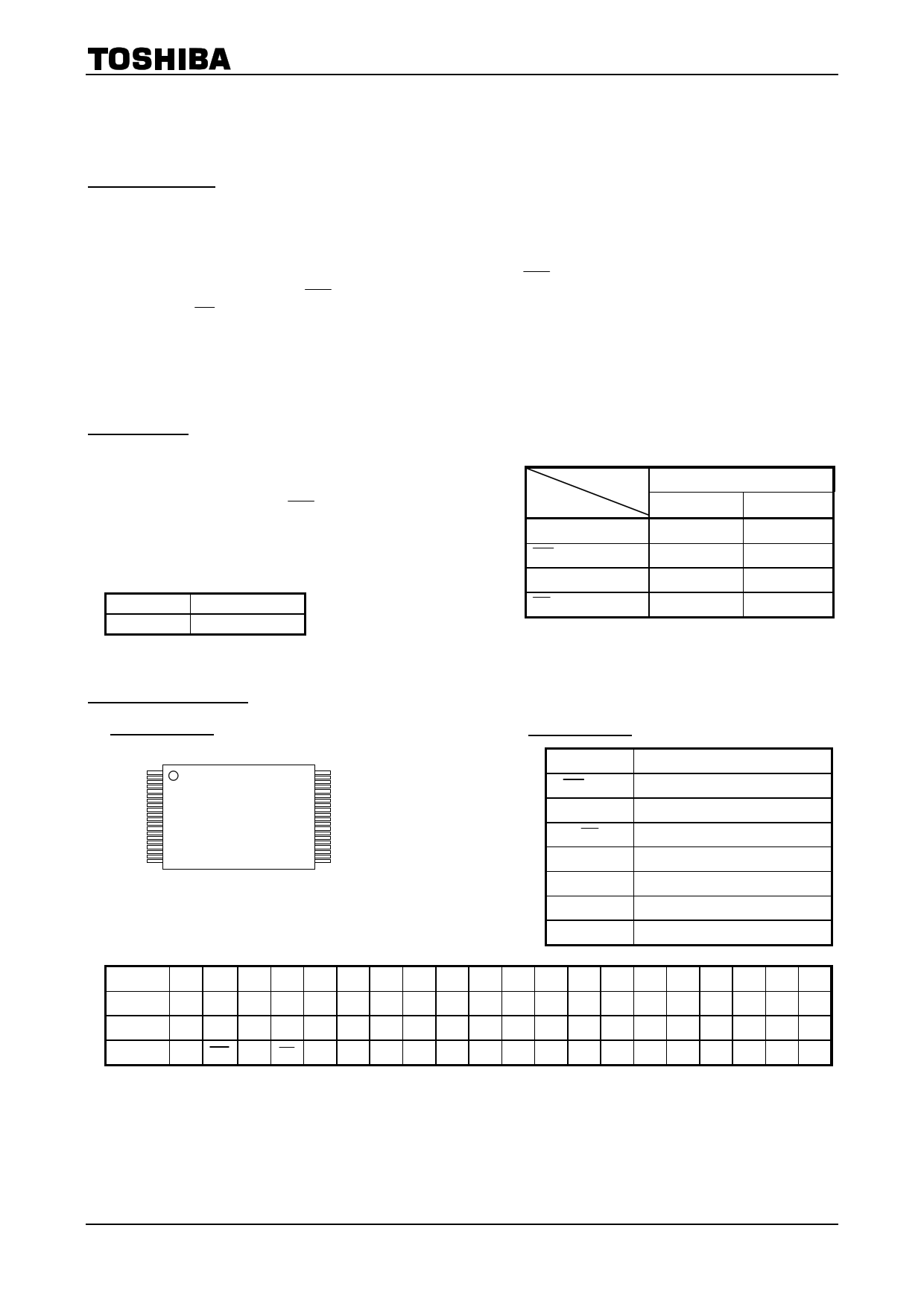
PIN ASSIGNMENT (TOP VIEW)
40 PIN TSOP
1 40
20 21
(Normal)
PIN NAMES
A0~A18
CE1 , CE2
R/W
OE
I/O1~I/O8
VDD
GND
NC
Address Inputs
Chip Enable
Read/Write Control
Output Enable
Data Inputs/Outputs
Power
Ground
No Connection
Pin No. 1 2 3 4 5 6 7 8 9 10 11 12 13 14 15 16 17 18 19 20
Pin Name A16 A15 A14 A13 A12 A11 A9 A8 R/W CE2 NC NC A18 A7 A6 A5 A4 A3 A2 A1
Pin No. 21 22 23 24 25 26 27 28 29 30 31 32 33 34 35 36 37 38 39 40
Pin Name A0 CE1 GND OE I/O1 I/O2 I/O3 I/O4 NC VDD VDD I/O5 I/O6 I/O7 I/O8 A10 NC NC GND A17
www.DataSheet4U.com
2003-08-06 1/11
1 page 
TC55V040AFT-55,-70
AC CHARACTERISTICS AND OPERATING CONDITIONS
(Ta = −40° to 85°C, VDD = 2.3 to 3.6 V)
READ CYCLE
SYMBOL
PARAMETER
tRC
tACC
tCO1
tCO2
tOE
tCOE
tOEE
tOD
tODO
tOH
Read Cycle Time
Address Access Time
Chip Enable( CE1 ) Access Time
Chip Enable(CE2) Access Time
Output Enable Access Time
Chip Enable Low to Output Active
Output Enable Low to Output Active
Chip Enable High to Output High-Z
Output Enable High to Output High-Z
Output Data Hold Time
TC55V040AFT
-55 -70
MIN MAX MIN MAX
70 85
70 85
70 85
70 85
35 45
55
00
30 35
30 35
10 10
UNIT
ns
WRITE CYCLE
SYMBOL
PARAMETER
tWC
tWP
tCW
tAS
tWR
tODW
tOEW
tDS
tDH
Write Cycle Time
Write Pulse Width
Chip Enable to End of Write
Address Setup Time
Write Recovery Time
R/W Low to Output High-Z
R/W High to Output Active
Data Setup Time
Data Hold Time
TC55V040AFT
-55 -70
MIN MAX MIN MAX
70 85
50 55
60 70
00
00
30 35
00
30 35
00
UNIT
ns
AC TEST CONDITIONS
PARAMETER
Output load
Input pulse level
Timing measurements
Reference level
tR, tF
TEST CONDITION
30 pF + 1 TTL Gate
VDD − 0.2 V, 0.2 V
VDD × 0.5
VDD × 0.5
5 ns
2003-08-06 5/11
5 Page 
TC55V040AFT-55,-70
RESTRICTIONS ON PRODUCT USE
030619EBA
• The information contained herein is subject to change without notice.
• The information contained herein is presented only as a guide for the applications of our products. No
responsibility is assumed by TOSHIBA for any infringements of patents or other rights of the third parties which
may result from its use. No license is granted by implication or otherwise under any patent or patent rights of
TOSHIBA or others.
• TOSHIBA is continually working to improve the quality and reliability of its products. Nevertheless, semiconductor
devices in general can malfunction or fail due to their inherent electrical sensitivity and vulnerability to physical
stress. It is the responsibility of the buyer, when utilizing TOSHIBA products, to comply with the standards of
safety in making a safe design for the entire system, and to avoid situations in which a malfunction or failure of
such TOSHIBA products could cause loss of human life, bodily injury or damage to property.
In developing your designs, please ensure that TOSHIBA products are used within specified operating ranges as
set forth in the most recent TOSHIBA products specifications. Also, please keep in mind the precautions and
conditions set forth in the “Handling Guide for Semiconductor Devices,” or “TOSHIBA Semiconductor Reliability
Handbook” etc..
• The TOSHIBA products listed in this document are intended for usage in general electronics applications
(computer, personal equipment, office equipment, measuring equipment, industrial robotics, domestic appliances,
etc.). These TOSHIBA products are neither intended nor warranted for usage in equipment that requires
extraordinarily high quality and/or reliability or a malfunction or failure of which may cause loss of human life or
bodily injury (“Unintended Usage”). Unintended Usage include atomic energy control instruments, airplane or
spaceship instruments, transportation instruments, traffic signal instruments, combustion control instruments,
medical instruments, all types of safety devices, etc.. Unintended Usage of TOSHIBA products listed in this
document shall be made at the customer’s own risk.
• The products described in this document are subject to the foreign exchange and foreign trade laws.
• TOSHIBA products should not be embedded to the downstream products which are prohibited to be produced
and sold, under any law and regulations.
2003-08-06 11/11
11 Page | ||
| Páginas | Total 11 Páginas | |
| PDF Descargar | [ Datasheet TC55V040AFT.PDF ] | |
Hoja de datos destacado
| Número de pieza | Descripción | Fabricantes |
| TC55V040AFT | 8-Bit FULL CMOS SRAM | Toshiba |
| TC55V040AFT | (TC55V040ATR/AFT) 8-Bit FULL CMOS SRAM | Toshiba |
| Número de pieza | Descripción | Fabricantes |
| SLA6805M | High Voltage 3 phase Motor Driver IC. |
Sanken |
| SDC1742 | 12- and 14-Bit Hybrid Synchro / Resolver-to-Digital Converters. |
Analog Devices |
|
DataSheet.es es una pagina web que funciona como un repositorio de manuales o hoja de datos de muchos de los productos más populares, |
| DataSheet.es | 2020 | Privacy Policy | Contacto | Buscar |