|
|
PDF AD5601 Data sheet ( Hoja de datos )
| Número de pieza | AD5601 | |
| Descripción | (AD5601 - AD5621) SPI Interface / SC70 Package / nanoDAC D/A | |
| Fabricantes | Analog Devices | |
| Logotipo |  |
|
Hay una vista previa y un enlace de descarga de AD5601 (archivo pdf) en la parte inferior de esta página. Total 17 Páginas | ||
|
No Preview Available !
om 2.7 V to 5.5 V, <100 µA, 8/10/12BitTM
PreliminatraySTehcehneitc4aUl D.acta nanoDAC D/A, SPAIDIn5t6e0rf1a/cAeD,5S6C1710/PAaDc5k6a2g1eFEATURES
a6-lead SC70 package
.DPower-down to <100 nA @ 3 V
wMicropower operation: max 100 µA @ 5 V
w2.7 V to 5.5 V power supply
wGuaranteed monotonic by design
Power-on-reset to 0 V with brownout detection
m3 power-down functions
oLow power serial interface with Schmitt-triggered inputs
On-chip output buffer amplifier, rail-to-rail operation
.cSYNC interrupt facility
Minimised Zero Code Error
AD5601 Buffered 8-Bit Dac in SC70
UB Version: ±0.5 LSB INL
t4AD5611 Buffered 10-Bit Dac in SC70
B Version: ±0.5 LSB INL, A Version: ±4 LSB INL
AD5621 Buffered 12-Bit Dac in SC70
eB Version: ±1 LSB INL , A Version: ±6 LSB INL
eAPPLICATIONS
hVoltage Level Setting
Portable battery-powered instruments
SDigital gain and offset adjustment
taProgrammable voltage and current sources
Programmable attenuators
aGENERAL DESCRIPTION
.DThe AD5601/AD5611/AD5621, members of the nanoDACTM family, are
single, 8/10/12-bit buffered voltage out DAC that operates from a single 2.7
V to +5.5 V supply consuming <100 µA at 5 V, and comes in a tiny SC70
package. Its on-chip precision output amplifier allows rail-to-rail output
wswing to be achieved. The AD5601/AD5611/AD5621 utilizes a versatile 3-
wire serial interface that operates at clock rates up to 30 MHz and is
wcompatible with SPI®, QSPI™, MICROWIRE™, and DSP interface standards.
mThe reference for AD5601/AD5611/AD5621 is derived from the power
w osupply inputs and thus gives the widest dynamic output range. The part
.cincorporates a power-on-reset circuit that ensures the DAC output powers
up to 0 V and remains there until a valid write takes place to the device. The
Upart contains a power-down feature that reduces the current consumption
t4of the device to <100 nA at 3 V and provides software selectable output
eloads while in power-down mode. The part is put into power-down mode
eover the serial interface. The low power consumption of this part in normal
hoperation makes it ideally suited to portable battery operated equipment.
ataSRev. PrB
.DInformation furnished by Analog Devices is believed to be accurate and reliable.
However, no responsibility is assumed by Analog Devices for its use, nor for any
infringements of patents or other rights of third parties that may result from its use.
wSpecifications subject to change without notice. No license is granted by implication
wor otherwise under any patent or patent rights of Analog Devices. Trademarks and
wregistered trademarks are the property of their respective owners.
FUNCTIONAL BLOCK DIAGRAM
Figure 1
RELATED DEVICES
Part Number
Description
AD5641
2.7 V to 5.5 V, <100 µA, 14 Bit nanoDACTM D/A, tiny
SC70 Package
The combination of small package and low power make these devices idea
for level setting requirements such as generating bias or control voltages in
space constrained and power sensitive applications
One Technology Way, P.O. Box 9106, Norwood, MA 02062-9106, U.S.A.
Tel: 781.329.4700
www.analog.com
Fax: 781.326.8703 © 2004 Analog Devices, Inc. All rights reserved.
1 page 
Preliminary Technical Data
AD5601/AD5611/AD5621
TIMING CHARACTERISTICS
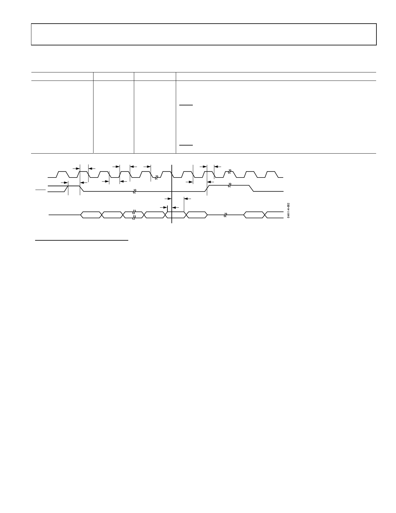
Table 2. VDD = 2.7 V to 5.5 V; all specifications TMIN to TMAX, unless otherwise noted. See Figure 2.
Parameter
Limit6
Unit
Test Conditions/Comments
t17
33
ns min
SCLK Cycle Time
t2
13
ns min
SCLK High Time
t3
12
ns min
SCLK Low Time
t4
13
ns min
SYNC to SCLK Falling Edge Setup Time
t5
5
ns min
Data Setup Time
t6
4.5
ns min
Data Hold Time
t7
0
ns min
SCLK Falling Edge to SYNC Rising Edge
t8
33
ns min
Minimum SYNC High Time
t9
13
ns min
SYNC Rising Edge to next SCLK Fall Ignore
SCLK
SYNC
DIN
t4
t8
D15
t2 t1
t3
t6
t5
D14 D2 D1
t9
t7
D0
D15 D14
Figure 2. Timing Diagram
6 All input signals are specified with tr = tf = 1 ns/V (10% to 90% of VDD) and timed from a voltage level of (VIL + VIH)/2.
7 Maximum SCLK frequency is 30 MHz.
Rev. PrB | Page 5 of 17
5 Page 
Preliminary Technical Data
AD5601/AD5611/AD5621
Figure 16. Power on Reset to 0 V
Figure 19. Exiting Power-Down
Figure 17. Digital to Analog Glitch Impulse
Figure 20. Harmonic Distortion on Digitally Generated Waveform.
Figure 18. Output Spectral Density 100k Bandwidth
Figure 21. 0.1 Hz to 10 Hz Noise Plot
Rev. PrB | Page 11 of 17
11 Page | ||
| Páginas | Total 17 Páginas | |
| PDF Descargar | [ Datasheet AD5601.PDF ] | |
Hoja de datos destacado
| Número de pieza | Descripción | Fabricantes |
| AD5601 | (AD5601 - AD5621) SPI Interface / SC70 Package / nanoDAC D/A | Analog Devices |
| AD5602 | 8-/10-/12-Bit nanoDACs | Analog Devices |
| Número de pieza | Descripción | Fabricantes |
| SLA6805M | High Voltage 3 phase Motor Driver IC. |
Sanken |
| SDC1742 | 12- and 14-Bit Hybrid Synchro / Resolver-to-Digital Converters. |
Analog Devices |
|
DataSheet.es es una pagina web que funciona como un repositorio de manuales o hoja de datos de muchos de los productos más populares, |
| DataSheet.es | 2020 | Privacy Policy | Contacto | Buscar |
