|
|
|
PDF ICS9147-01 Data sheet ( Hoja de datos )
| Número de pieza | ICS9147-01 | |
| Descripción | Frequency Generator & Integrated Buffers | |
| Fabricantes | Integrated Circuit Systems | |
| Logotipo | ||
Hay una vista previa y un enlace de descarga de ICS9147-01 (archivo pdf) en la parte inferior de esta página. Total 11 Páginas | ||
|
No Preview Available !
Integrated
Circuit
Systems, Inc.
ICS9147- 01
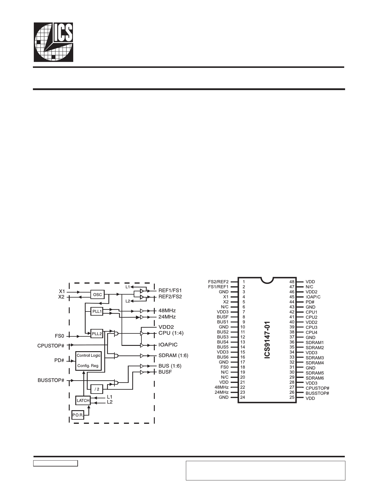
Frequency Generator & Integrated Buffers for PENTIUMTM
General Description
The ICS9147-01 generates all clocks required for high
speed RISC or CISC microprocessor systems such as Intel
PentiumPro. Two bidirectional I/O pins (FS1,FS2) are latched
at power-on to the functionality table, with FS0 selectable
in real-time to toggle between conditions. The inputs
provide for tristate and test mode conditions to aid in
system level testing. These multiplying factors can be
customized for specific applications. Glitch-free stop
clockcontrols are provided for CPU clocks and BUS clocks.
High drive BUS and SDRAM outputs typically provide
greater than 1 V/ns slew rate into 30 pF loads. CPU outputs
typically provide better than 1V/ns slew rate into 20 pF
loads while maintaining 50 ±5% duty cycle. The REF clock
outputs typically provide better than 0.5V/ns slew rates.
Seperate buffers supply pins VDD2 allow for 3.3V or
reduced voltage swing (from 2.9 to 2.5V) for CPU (1:4) and
IOAPIC outputs.
Features
• Four copies of CPU clock
• Six SDRAM (3.3 V TTL), usable as AGP clocks
• Seven copies of BUS clock (synchronous with CPU
clock/2 or CPU/2.5 for 75 and 83.3 MHz CPU)
• CPU clocks to BUS clocks skew 1-4ns (CPU early)
• One IOAPIC clock @14.31818 MHz
• Two copies of Ref. clock @14.31818 MHz
• One each 48/ 24 MHz (3.3 V TTL)
• This device is configured into the Mobile mode for
power management of Intel 430 TX
• Ref. 14.31818 MHz Xtal oscillator input
• Separate 66/60 MHz select pin (LSB of select pins)
• Separate VDD2 for four CPU and single IOAPIC output
buffers to allow 2.5V output (or Std. Vdd)
• Power Management Control Input pins
• 3.0V – 3.7V supply range w/2.5V compatible outputs
• 48-pin SSOP package
Block Diagram
Pin Configuration
9147-01Rev B 04/25/01
48-Pin SSOP
Pentium is a trademark of Intel Corporation
ICS reserves the right to make changes in the device data identified in this publication
without further notice. ICS advises its customers to obtain the latest version of all
device data to verify that any information being relied upon by the customer is current
and accurate.
1 page 
ICS9147- 01
Notes:
1. All timing is referenced to the Internal BUS clock (defined as inside the ICS9147 device.)
2. BUSSTOP# is an asynchronous input, and metastable conditions may exist. This signal is required to be
synchronized inside the ICS9147.
3. All other clocks continue to run undisturbed.
4. PD# and CPUSTOP# are shown in a high (true) state.
PD# Timing Diagram
The power down selection is used to put the part into a very low power state without turning off the power to the part.
PD# is an asynchronous active low input. This signal is synchronized internal by the ICS9147-01 prior to its control
action of powering down the clock synthesizer. PD# is an asynchronous function for powering up the system. Internal
clocks will not be running after the device is put in power down state. When PD# is active (low) all clocks are driven to
a low state and held prior to turning off the VCOs and the Crystal oscillator. The power on latency is guaranteed to be
less than 3mS. The power down latency is less than three CPU clock cycles. BUSSTOP# and CPUSTOP# are don’t care
signals during the power down operations.
Notes:
1. All timing is referenced to the Internal CPU clock (defined as inside the ICS9147 device).
2. PD# is an asynchronous input and metastable conditions may exist. This signal is synchronized inside the ICS9147.
3. The shaded sections on the VCO and the Crystal signals indicate an active clock is being generated.
5
5 Page 
ICS9147- 01
N
INDEX
AREA
12
D
c
E1 E
L
h x 45°
a
A
A1
-C-
e
b
SEATING
PLANE
.10 (.004) C
300 mil SSOP Package
SYMBOL
A
A1
b
c
D
E
E1
e
h
L
N
α
In Millimeters
COMMON DIMENSIONS
MIN MAX
2.41 2.80
0.20 0.40
0.20 0.34
0.13 0.25
SEE VARIATIONS
10.03
10.68
7.40 7.60
0.635 BASIC
0.38 0.64
0.50 1.02
SEE VARIATIONS
0° 8°
In Inches
COMMON DIMENSIONS
MIN MAX
.095 .110
.008 .016
.008 .0135
.005 .010
SEE VARIATIONS
.395 .420
.291 .299
0.025 BASIC
.015 .025
.020 .040
SEE VARIATIONS
0° 8°
VARIATIONS
N
D mm.
MIN MAX
48
15.75
16.00
Reference Doc.: JEDEC Publication 95, MO-118
10-0034
D (inch)
MIN MAX
.620 .630
Ordering Information
ICS9147F-01
Example:
ICS XXXX F - PPP
Pattern Number (2 or 3 digit number for parts with ROM code patterns)
Package Type
F=SSOP
Device Type (consists of 3 or 4 digit numbers)
Prefix
ICS = Standard Device
11
11 Page | ||
| Páginas | Total 11 Páginas | |
| PDF Descargar | [ Datasheet ICS9147-01.PDF ] | |
Hoja de datos destacado
| Número de pieza | Descripción | Fabricantes |
| ICS9147-01 | Frequency Generator & Integrated Buffers | Integrated Circuit Systems |
| ICS9147-03 | Frequency Generator & Integrated Buffers | Integrated Circuit Systems |
| ICS9147-06 | Frequency Generator & Integrated Buffers | Integrated Circuit Systems |
| ICS9147-09 | Frequency Generator & Integrated Buffers | Integrated Circuit Systems |
| Número de pieza | Descripción | Fabricantes |
| SLA6805M | High Voltage 3 phase Motor Driver IC. |
Sanken |
| SDC1742 | 12- and 14-Bit Hybrid Synchro / Resolver-to-Digital Converters. |
Analog Devices |
|
DataSheet.es es una pagina web que funciona como un repositorio de manuales o hoja de datos de muchos de los productos más populares, |
| DataSheet.es | 2020 | Privacy Policy | Contacto | Buscar |