|
|
PDF ICS9147-06 Data sheet ( Hoja de datos )
| Número de pieza | ICS9147-06 | |
| Descripción | Frequency Generator & Integrated Buffers | |
| Fabricantes | Integrated Circuit Systems | |
| Logotipo |  |
|
Hay una vista previa y un enlace de descarga de ICS9147-06 (archivo pdf) en la parte inferior de esta página. Total 6 Páginas | ||
|
No Preview Available !
Integrated
Circuit
Systems, Inc.
ICS9147-06
Frequency Generator & Integrated Buffers for PENTIUMTM
General Description
The ICS9147-06 generates all clocks required for high
speed RISC or CISC microprocessor systems such as Intel
PentiumPro. Two different reference frequency multiplying
factors are externally selectable with smooth frequency
transitions. Glitch-free Stop clock control is provided for
CPU and BUS clocks. Complete chip low current mode is
achieved with the Power Down# pin.
High drive BUS outputs typically provide greater than 1V/
ns slew rate into 30 pF loads. CPU outputs typically provide
better than 1V/ns slew rate into 20 pF loads while
maintaining 50±5% duty cycle. The REF and IOAPIC clock
outputs typically provide better than 0.5V/ns slew rates.
Separate buffer supply pins VDDL allow for nominal 3.3V
voltage or reduced voltage swing (from 2.9 to 2.5V) for
CPU (1:4) and IOAPIC outputs.
Block Diagram
Features
Generates five processor, eight bus, four 14.31818 MHz,
two 48 MHz clocks for USB support and one 24 MHz
clock.
CPU to BUS clock skew 1 to 4ns (CPU early)
Synchronous clocks skew matched to 250ps window on
CPU and 500ps window on BUS.
Selectable multiplying ratios
Glitch free stop clock controls CPUEN and BUSEN
3.0V 3.7V supply range, 2.5V to VDD supply range for
CPU (1:4) clocks and IOAPIC clock.
48-pin SSOP package
Pin Configuration
9147- 06 RevA 5/29/97P
48-Pin SSOP
Pentium is a trademark of Intel Corporation
ICS reserves the right to make changes in the device data identified in this publication
without further notice. ICS advises its customers to obtain the latest version of all
device data to verify that any information being relied upon by the customer is current
and accurate.
1 page 
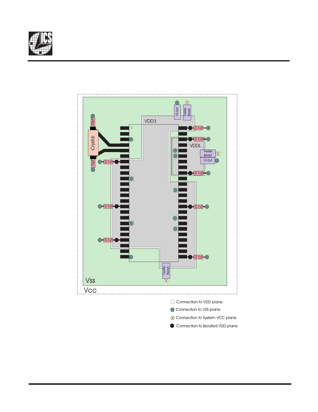
Recommended PCB Layout for ICS9147-06
ICS9147-06
NOTE:
This PCB Layout is based on a 4 layer board with an internal Ground (common) and Vcc plane. Placement of
components will depend on routing of signal trace. The 0.1uf Capacitors should be placed as close as possible
to the Power pins. Placement on the backside of the board is also possible. The Ferrite Beads can be replaced
with 10-15ohm Resistors. For best results, use a Fixed Voltage Regulator between the main (board) Vcc and the
different Vdd planes.
5
5 Page | ||
| Páginas | Total 6 Páginas | |
| PDF Descargar | [ Datasheet ICS9147-06.PDF ] | |
Hoja de datos destacado
| Número de pieza | Descripción | Fabricantes |
| ICS9147-01 | Frequency Generator & Integrated Buffers | Integrated Circuit Systems |
| ICS9147-03 | Frequency Generator & Integrated Buffers | Integrated Circuit Systems |
| ICS9147-06 | Frequency Generator & Integrated Buffers | Integrated Circuit Systems |
| ICS9147-09 | Frequency Generator & Integrated Buffers | Integrated Circuit Systems |
| Número de pieza | Descripción | Fabricantes |
| SLA6805M | High Voltage 3 phase Motor Driver IC. |
Sanken |
| SDC1742 | 12- and 14-Bit Hybrid Synchro / Resolver-to-Digital Converters. |
Analog Devices |
|
DataSheet.es es una pagina web que funciona como un repositorio de manuales o hoja de datos de muchos de los productos más populares, |
| DataSheet.es | 2020 | Privacy Policy | Contacto | Buscar |
