|
|
|
PDF ICS9147-09 Data sheet ( Hoja de datos )
| Número de pieza | ICS9147-09 | |
| Descripción | Frequency Generator & Integrated Buffers | |
| Fabricantes | Integrated Circuit Systems | |
| Logotipo | ||
Hay una vista previa y un enlace de descarga de ICS9147-09 (archivo pdf) en la parte inferior de esta página. Total 9 Páginas | ||
|
No Preview Available !
Integrated
Circuit
Systems, Inc.
ICS9147- 09
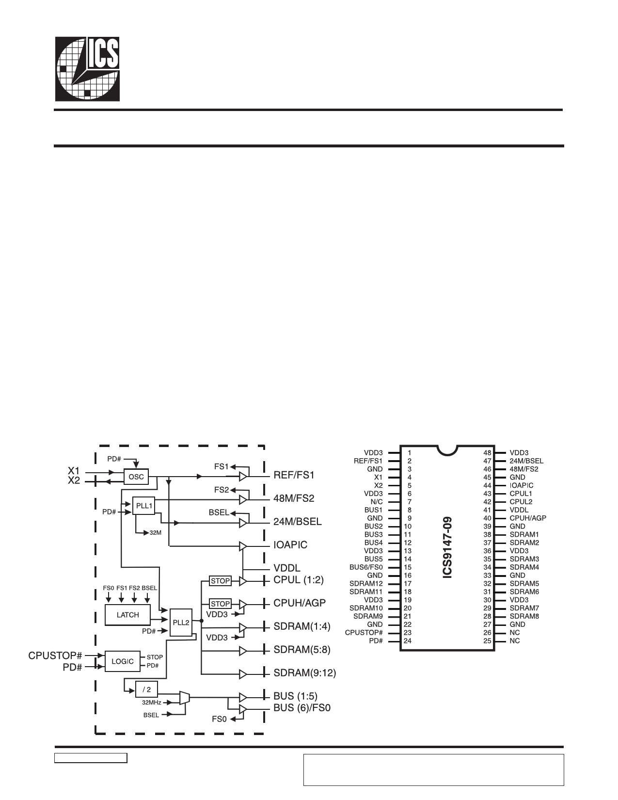
Frequency Generator & Integrated Buffers for 686 Series CPUs
General Description
The ICS9147-09 generates all clocks required for high
speed RISC or CISC microprocessor systems such as Intel
PentiumPro,AMD or Cyrix processors. Four bidirectional I/O
pins (FS0, FS1, FS2, BSEL) are latched at power-on to the
functionality table. The Six BUS clocks can be selected as
either synchronous at 1/2 CPU speed or asynchronous at
32MHz selected by BSEL latched input.The inputs provide
for tristate and test mode conditions to aid in system level
testing.These multiplying factors can be customized for
specific applications. Glitch-free stop clock controls
provided for CPU.
High drive BUS and SDRAM outputs typically provide
greater than 1 V/ns slew rate into 30 pF loads. CPU outputs
typically provide better than 1V/ns slew rate into 20pF
loads while maintaining 50±5% duty cycle. The REF clock
outputs typically provide better than 0.5V/ns slew rates.
Seperate buffer supply pin VDDL allows for nominal 3.3V
voltage or reduced voltage swing (from 2.9 to 2.5V) for
CPUL (1:2) and IOAPIC outputs.
Features
Total of 15 CPU speed clocks:
- Two copies of CPU clock with VDDL (2.5 to 3.3V)
- Twelve (12) SDRAM (3.3v) plus one
CPUH/AGP (3.3V) clocks
Six copies of BUS clock (synchronous with CPU clock/2 or
asynchronous 32 MHz)
250ps output skew window for CPU andSDRAM clocks
and 500ps window BUS clocks. CPU clocks to
BUSclocks skew 1-4ns (CPU early)
Two copies of Ref. clock @14.31818 MHz (One driven
by VDDL as IOAPIC)
One 48 MHz (3.3 V TTL) for USB support and single
24 MHz.
Separate VDDL for CPUL (1:2) clock buffers and
IOAPIC to allow 2.5V output (or Std. Vdd)
3.0V 3.7V supply range w/2.5V compatible outputs
48-pin SSOP package
Block Diagram
Pin Configuration
9147-09 Rev A 10/2897P
48-Pin SSOP
Pentium is a trademark of Intel Corporation
ICS reserves the right to make changes in the device data identified in this
publication without further notice. ICS advises its customers to obtain the latest
version of all device data to verify that any information being relied upon by the
customer is current and accurate.
1 page 
ICS9147- 09
Electrical Characteristics at 3.3V
VDD = 3.0 3.7 V, TA = 0 70° C unless otherwise stated
PARAMETER
Rise Time1
Fall Time1
Rise Time1
Fall Time1
Rise Time1
Fall Time1
Duty Cycle1
Duty Cycle1
Jitter, One Sigma1
Jitter, Absolute1
Jitter, One Sigma1
Jitter, Absolute1
Jitter, Cycle to Cycle1
Jitter, Cycle to Cycle1
Input Frequency1
Ratio of nominal to output
frequency
Logic Input Capacitance1
Crystal Oscillator Capacitance1, 2
Power-on Time1
Clock Skew Window1
Clock Skew Window1
Clock Skew Window1
Clock Skew Window1
Clock Skew Window1
SYMBOL
Tr1
Tf1
Tr3
Tf3
Tr4
Tf4
Dt
DT2
Tjis1
Tjab1
Tjis2
Tjab2
Tcc1
Tcc2
Fi
Fout1
CIN
CINX
ton
Tsk1
Tsk2
Tsk3
Tsk4
Tsk5
AC Characteristics
TEST CONDITIONS
20pF load, 0.8 to 2.0V
CPU, SDRAM, BUS & REF
20pF load, 2.0 to 0.8V
CPU, SDRAM, BUS & REF
20pF load, 0.8 to 2.0V
fixed 20 & 48 clocks
20pF load, 2.0 to 0.8V
fixed 20 & 48 clocks
20pF load, 0.4 to 2.0V , CPUL with
VDDL = 2.5V
20pF load, 2.0 to 0.4V, CPUL with
VDDL = 2.5V
20pF load @ VOUT=1.4V
All clocks except 48MHz and REF
20pF load @ VOUT=1.4V
48MHz and REF outputs
CPU & BUS Clocks; Load=20pF,
SDRAM; Load = 30pF, VDDL = 3.3
or 2.5V
FOUT=25 MHz, BSEL=1
CPU & BUS Clocks; Load=20pF,
SDRAM; Load = 30pF, VDDL = 3.3
or 2.5V
FOUT≥25 MHz, BSEL=1
Fixed CLK; Load=20pF
Fixed CLK; Load=20pF
CPU Clocks, Load=20pF BSEL=1
CPU Clocks, Load=20pF BSEL=1
VDDL=2.5V
With input driven at 14.31818MHz to
20.0, 48.0MHz
Logic input pins
X1, X2 pins
From VDD=1.6V to 1st crossing of
66.6 MHz VDD supply ramp < 40ms
CPU to CPU or SDRAM;
Load=20pF; @1.4V
(Same VDD)
BUS to BUS, SDRAM to SDRAM;
Load=20pF; @1.4V
CPU to BUS; Load=20pF; @1.4V
(CPU is early)
CPUL to BUS, VDDL=2.5V
Vth=1.25, CPUL (BUS Vth=1.4V)
SDRAM, CPUH (@3.3V, Vth=1.4V)
to CPUL (@2.5V Vth=1.25V)
Load=20pF
(2.5V CPUL is late)
MIN
-
-
-
-
-
-
47
40
-
-250
-
-5
12.0
-1
-
2
-
-
-
1.6
0.50
100
Note 1: Parameter is guaranteed by design and characterization. Not 100% tested in production.
TYP
0.9
0.8
0.9
1.1
2.0
1.6
52
50
50
-
1
2
-
-
14.318
-0.1
5
4
2.5
150
300
2.1
1.50
600
MAX
1.5
1.4
1.5
1.5
2.5
2.5
57
60
150
250
3
5
250
350
16.0
+1
-
6
4.5
250
500
4.6
3.0
850
UNITS
ns
ns
ns
ns
ns
ns
%
%
ps
ps
%
%
ps
ps
MHz
ppm
pF
pF
ms
ps
ps
ns
ns
ps
5
5 Page | ||
| Páginas | Total 9 Páginas | |
| PDF Descargar | [ Datasheet ICS9147-09.PDF ] | |
Hoja de datos destacado
| Número de pieza | Descripción | Fabricantes |
| ICS9147-01 | Frequency Generator & Integrated Buffers | Integrated Circuit Systems |
| ICS9147-03 | Frequency Generator & Integrated Buffers | Integrated Circuit Systems |
| ICS9147-06 | Frequency Generator & Integrated Buffers | Integrated Circuit Systems |
| ICS9147-09 | Frequency Generator & Integrated Buffers | Integrated Circuit Systems |
| Número de pieza | Descripción | Fabricantes |
| SLA6805M | High Voltage 3 phase Motor Driver IC. |
Sanken |
| SDC1742 | 12- and 14-Bit Hybrid Synchro / Resolver-to-Digital Converters. |
Analog Devices |
|
DataSheet.es es una pagina web que funciona como un repositorio de manuales o hoja de datos de muchos de los productos más populares, |
| DataSheet.es | 2020 | Privacy Policy | Contacto | Buscar |