|
|
|
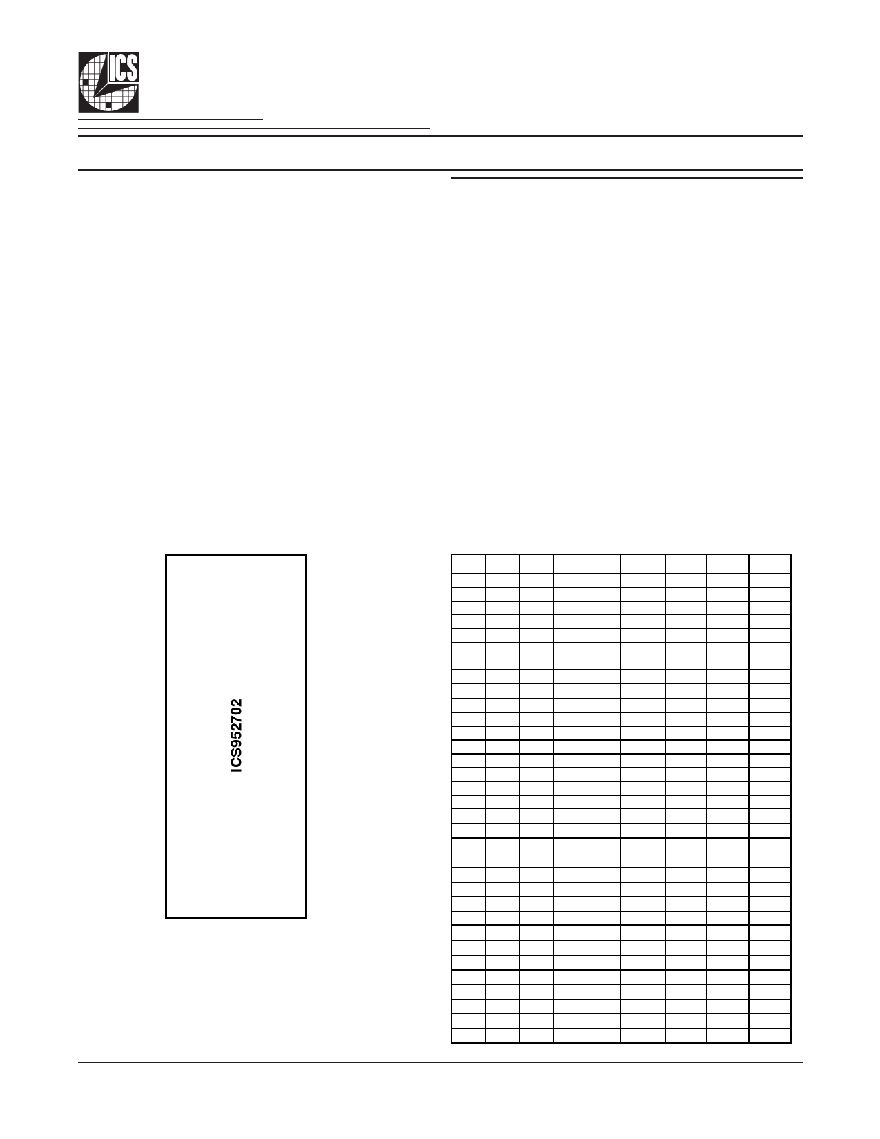
PDF ICS952702 Data sheet ( Hoja de datos )
| Número de pieza | ICS952702 | |
| Descripción | Programmable Timing Control Hub for K7 System | |
| Fabricantes | Integrated Circuit Systems | |
| Logotipo | ||
Hay una vista previa y un enlace de descarga de ICS952702 (archivo pdf) en la parte inferior de esta página. Total 17 Páginas | ||
|
No Preview Available !
Integrated
Circuit
Systems, Inc.
ICS952702
Programmable Timing Control Hub for K7TM System
Recommended Application:
SiS746/746FX style chipset
Output Features:
• 1 - Pair of differential open drain CPU outputs
• 1 - Single-ended open drain CPU output
• 8 - PCICLK @ 3.3V including 2 PCI clock free running
• 2 - AGPCLK @ 3.3V
• 3 - REF @ 3.3V
• 2 - ZCLK @ 3.3V
• 2 - IOAPIC @ 2.5V
• 1 - 12_48MHz @ 3.3V
• 1 - 24_48MHz @ 3.3V
Key Specifications:
• CPU Output Jitter <250ps
• AGP Output Jitter <250ps
• ZCLK Output Jitter <250ps
• PCI Output Jitter <500ps
• CPU-AGP/PCI/ZCLK skew: 2.5ns~3.5ns
Features/Benefits:
• Selectable synchronous/asynchronous AGP/PCI
frequency
• Programmable output frequency.
• Programmable output divider ratios.
• Programmable output rise/fall time.
• Programmable output skew.
• Programmable spread percentage for EMI control.
• Watchdog timer technology to reset system
if system malfunctions.
• Programmable watch dog safe frequency.
• Support I2C Index read/write and block read/write
operations.
• Uses external 14.318MHz reference or XTAL input.
Pin Configuration
Functionality
VDDREF 1
48 VDDLAPIC
**FS0/REF0 2
47 IOAPIC1
**FS1/REF1 3
46 IOAPIC0
**FS4/REF2 4
45 GNDAPIC
GNDREF 5
44 CPU_STOP#*
X1 6
43 CPUCLKODT1
X2 7
42 RESET#
GNDZ 8
41 GNDCPU
ZCLK0 9
40 CPUCLKODT0
ZCLK1 10
39 CPUCLKODC0
VDDZ 11
38 VDDCPU
*PCI_STOP# 12
37 AGND
VDDPCI 13
36 AVDD
**FS2/PCICLK_F0 14
35 SCLK
*FS3/PCICLK_F1 15
34 SDATA
PCICLK0 16
33 PD#*
PCICLK1 17
GNDPCI 18
32 GNDAGP
31 AGPCLK0
VDDPCI 19
30 AGPCLK1
PCICLK2 20
29 VDDAGP
PCICLK3 21
28 AVDD48
PCICLK4 22
27 12_48MHz/SEL12#_48MHz*
PCICLK5 23
26 24_48MHz/SEL24#_48MHz**
GNDPCI 24
25 GND48
48-SSOP
* Internal Pull-Up Resistor
** Internal Pull-Down Resistor
0795D—05/06/05
Bit4 Bit3 Bit2 Bit1 Bit0 CPU ZCLK AGP
FS4 FS3 FS2 FS1 FS0 MHz MHz MHz
0 0 0 0 0 200.00 133.33 66.67
0 0 0 0 1 200.99 133.99 67.00
0 0 0 1 0 200.00 66.67 66.67
0 0 0 1 1 206.00 137.33 68.67
0 0 1 0 0 133.33 133.33 66.67
0 0 1 0 1 214.00 142.66 71.33
0 0 1 1 0 218.00 145.33 72.67
0 0 1 1 1 222.00 148.00 74.00
0 1 0 0 0 100.00 133.33 66.67
0 1 0 0 1 100.99 134.65 67.33
0 1 0 1 0 100.00 66.67 66.67
0 1 0 1 1 103.00 137.33 68.67
0 1 1 0 0 100.00 133.33 66.67
0 1 1 0 1 107.00 142.66 71.33
0 1 1 1 0 109.00 145.33 72.67
0 1 1 1 1 111.00 148.00 74.00
1 0 0 0 0 166.67 133.33 66.67
1 0 0 0 1 166.99 133.59 66.80
1 0 0 1 0 166.67 66.67 66.67
1 0 0 1 1 171.67 137.33 68.67
1 0 1 0 0 175.00 140.00 70.00
1 0 1 0 1 178.34 142.66 71.33
1 0 1 1 0 181.67 145.33 72.67
1 0 1 1 1 185.00 148.00 74.00
1 1 0 0 0 133.33 133.33 66.67
1 1 0 0 1 133.99 133.99 67.00
1 1 0 1 0 133.33 66.67 66.67
1 1 0 1 1 137.33 137.33 68.67
1 1 1 0 0 140.00 140.00 70.00
1 1 1 0 1 142.66 142.66 71.33
1 1 1 1 0 145.33 145.33 72.67
1 1 1 1 1 148.00 148.00 74.00
PCI
MHz
33.33
33.50
33.33
34.33
33.33
35.67
36.33
37.00
33.33
33.66
33.33
34.33
33.33
35.67
36.33
37.00
33.33
33.40
33.33
34.33
35.00
35.67
36.33
37.00
33.33
33.50
33.33
34.33
35.00
35.67
36.33
37.00
1 page 
Integrated
Circuit
Systems, Inc.
Table 1: Frequency Selection Table
FSA FSB
Bit4 Bit3 Bit2 Bit1 Bit0 CPU
FS4 FS3 FS2 FS1 FS0 MHz
0 0 0 0 0 200.00
0 0 0 0 1 200.99
0 0 0 1 0 200.00
0 0 0 1 1 206.00
0 0 1 0 0 133.33
0 0 1 0 1 214.00
0 0 1 1 0 218.00
0 0 1 1 1 222.00
0 1 0 0 0 100.00
0 1 0 0 1 100.99
0 1 0 1 0 100.00
0 1 0 1 1 103.00
0 1 1 0 0 100.00
0 1 1 0 1 107.00
0 1 1 1 0 109.00
0 1 1 1 1 111.00
1 0 0 0 0 166.67
1 0 0 0 1 166.99
1 0 0 1 0 166.67
1 0 0 1 1 171.67
1 0 1 0 0 175.00
1 0 1 0 1 178.34
1 0 1 1 0 181.67
1 0 1 1 1 185.00
1 1 0 0 0 133.33
1 1 0 0 1 133.99
1 1 0 1 0 133.33
1 1 0 1 1 137.33
1 1 1 0 0 140.00
1 1 1 0 1 142.66
1 1 1 1 0 145.33
1 1 1 1 1 148.00
ZCLK
MHz
133.33
133.99
66.67
137.33
133.33
142.66
145.33
148.00
133.33
134.65
66.67
137.33
133.33
142.66
145.33
148.00
133.33
133.59
66.67
137.33
140.00
142.66
145.33
148.00
133.33
133.99
66.67
137.33
140.00
142.66
145.33
148.00
AGP
MHz
66.67
67.00
66.67
68.67
66.67
71.33
72.67
74.00
66.67
67.33
66.67
68.67
66.67
71.33
72.67
74.00
66.67
66.80
66.67
68.67
70.00
71.33
72.67
74.00
66.67
67.00
66.67
68.67
70.00
71.33
72.67
74.00
PCI
MHz
33.33
33.50
33.33
34.33
33.33
35.67
36.33
37.00
33.33
33.66
33.33
34.33
33.33
35.67
36.33
37.00
33.33
33.40
33.33
34.33
35.00
35.67
36.33
37.00
33.33
33.50
33.33
34.33
35.00
35.67
36.33
37.00
Spread %
+/-0.35% center
+/-0.35% center
+/-0.35% center
+/-0.35% center
+/-0.35% center
+/-0.35% center
+/-0.35% center
+/-0.35% center
+/-0.35% center
+/-0.35% center
+/-0.35% center
+/-0.35% center
+/-0.35% center
+/-0.35% center
+/-0.35% center
+/-0.35% center
+/-0.35% center
+/-0.35% center
+/-0.35% center
+/-0.35% center
+/-0.35% center
+/-0.35% center
+/-0.35% center
+/-0.35% center
+/-0.35% center
+/-0.35% center
+/-0.35% center
+/-0.35% center
+/-0.35% center
+/-0.35% center
+/-0.35% center
+/-0.35% center
ICS952702
0795D—05/06/05
5
5 Page 
Integrated
Circuit
Systems, Inc.
Electrical Characteristics - CPUCLKODC/T
TA = 0 - 70°C; VDD = 1.7 V +/-5%; CL = 5 pF (unless otherwise stated)
PARAMETER
SYMBOL
CONDITIONS
Output High Voltage VOH2B Termination to Vpull-up(external)
Output Low Voltage VOL2B Termination to Vpull-up(external)
Output Low Current
IOL2B
VOL = 0.3 V
Rise Time1
tr2B VOL = 20%, VOH = 80%
Fall Time1
Differential voltage-
AC1
Differential voltage-
DC1
tf2B
VDIF
VDIF
VOH = 80%, VOL = 20%,
Differential Crossover
Voltage1
VX
Duty Cycle1
dt2B VT = 50%
Skew1
tsk2B
VT = 50%
Jitter Diff, Cycle-to-
cycle1
tjcyc-cyc2B VT = VX
Jitter SE, Cycle-to-
cycle1
tjcyc-cyc2B VT = 1.0V
Jitter, Absolute1
tjabs2B
VT = 50%
Notes:
1 - Guaranteed by design, not 100% tested in production.
Electrical Characteristics - PCICLK
TA = 0 - 70°C; VDD = 3.3 V,+/-5%; CL = 30 pF
PARAMETER
SYMBOL
CONDITIONS
Output High Voltage
VOH1 IOH = -18 mA
Output Low Voltage
VOL1
IOL = 9.4 mA
Output High Current
IOH1 VOH = 2.0 V
Output Low Current
Rise Time1
Fall Time1
Duty Cycle1
Skew1
IOL1 VOL = 0.8 V
tr1 VOL = 0.4 V, VOH = 2.4 V
tf1 VOH = 2.4 V, VOL = 0.4 V
dt1 VT = 1.5 V
tsk1 VT = 1.5 V
Jitter
tjcyc-cyc1
tjabs1
VT = 1.5 V
VT = 1.5 V
1Guaranteed by design, not 100% tested in production.
ICS952702
MIN TYP MAX UNITS
1 1.2 V
0.4 V
18 mA
0.38 0.9 ns
0.44 0.9 ns
0.4 V
0.2 V
550 1200 1250 mV
45 51.5 55
%
140 200 ps
60 250 ps
100 250
-250 250
ps
ps
MIN TYP MAX UNITS
2.1 V
0.4 V
-22 mA
16 57 mA
2.25 2.5 ns
2.1 2.5 ns
45 50 55 %
170 500 ps
150 500 ps
500 ps
0795D—05/06/05
11
11 Page | ||
| Páginas | Total 17 Páginas | |
| PDF Descargar | [ Datasheet ICS952702.PDF ] | |
Hoja de datos destacado
| Número de pieza | Descripción | Fabricantes |
| ICS952702 | Programmable Timing Control Hub for K7 System | Integrated Circuit Systems |
| ICS952703 | Programmable Timing Control Hub for K7 System | Integrated Circuit Systems |
| Número de pieza | Descripción | Fabricantes |
| SLA6805M | High Voltage 3 phase Motor Driver IC. |
Sanken |
| SDC1742 | 12- and 14-Bit Hybrid Synchro / Resolver-to-Digital Converters. |
Analog Devices |
|
DataSheet.es es una pagina web que funciona como un repositorio de manuales o hoja de datos de muchos de los productos más populares, |
| DataSheet.es | 2020 | Privacy Policy | Contacto | Buscar |