|
|
|
PDF DP8419 Data sheet ( Hoja de datos )
| Número de pieza | DP8419 | |
| Descripción | (DP8417 - DP8419) 64k / 256k Dynamic RAM Controller/Drivers | |
| Fabricantes | National Semiconductor | |
| Logotipo | ||
Hay una vista previa y un enlace de descarga de DP8419 (archivo pdf) en la parte inferior de esta página. Total 28 Páginas | ||
|
No Preview Available !
PRELIMINARY
August 1989
DP8417 NS32817 8418 32818 8419 32819 8419X
32819X 64k 256k Dynamic RAM Controller Drivers
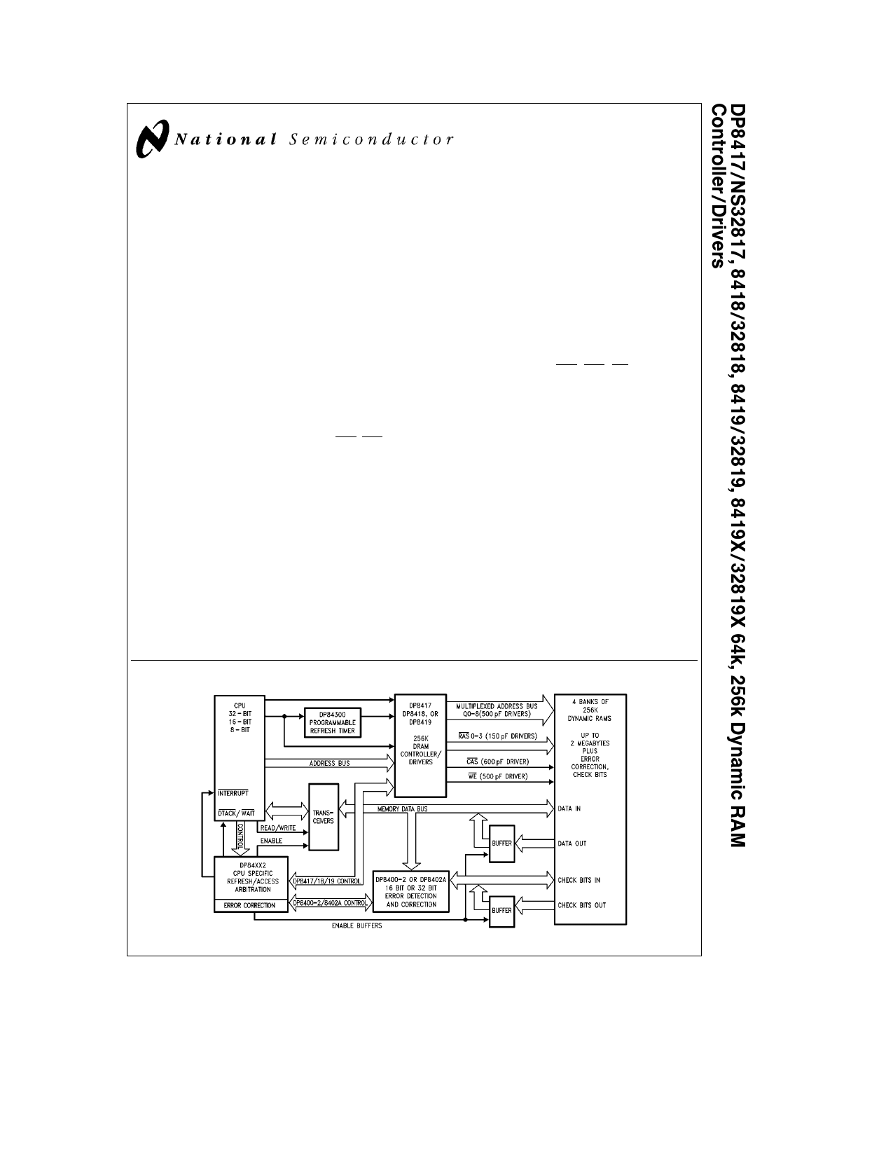
General Description
The DP8417 8418 8419 8419X represent a family of 256k
DRAM Controller Drivers which are designed to provide
‘‘No-Waitstate’’ CPU interface to Dynamic RAM arrays of up
to 2 Mbytes and larger Each device offers slight functional
variations of the DP8419 design which are tailored for differ-
ent system requirements All family members are fabricated
using National’s new oxide isolated Advanced Low power
Schottky (ALS) process and use design techniques which
enable them to significantly out-perform all other LSI or dis-
crete alternatives in speed level of integration and power
consumption
Each device integrates the following critical 256k DRAM
controller functions on a single monolithic device ultra pre-
cise delay line 9-bit refresh counter fall-through row col-
umn and bank select input latches Row Column address
muxing logic on-board high capacitive-load RAS CAS and
Write Enable Address output drivers and precise control
signal timing for all the above
There are four device options of the basic DP8419 Control-
ler The DP8417 is pin and function compatible with the
DP8419 except that its outputs are TRI-STATE The
DP8418 changes one pin and is specifically designed to
offer an optimum interface to 32 bit microprocessors The
DP8419X is functionally identical to the DP8419 but is avail-
able in a 52-pin DIP package which is upward pin compati-
ble with National’s new DP8429D 1 Mbit DRAM Controller
Driver
Each device is available in plastic DIP Ceramic DIP and
Plastic Chip Carrier (PCC) packaging (Continued)
TRI-STATE is a registered trademark of National Semiconductor Corp
PAL is a registered trademark of and used under license with Monolithic Memories Inc
Operational Features
Y Makes DRAM Interface and refresh tasks appear virtu-
ally transparent to the CPU making DRAMs as easy to
use as static RAMs
Y Specifically designed to eliminate CPU wait states up to
10 MHz or beyond
Y Eliminates 15 to 20 SSI MSI components for significant
board real estate reduction system power savings and
the elimination of chip-to-chip AC skewing
Y On-board ultra precise delay line
Y On-board high capacitive RAS CAS WE and address
drivers (specified driving 88 DRAMs directly)
Y AC specified for directly addressing up to 8 Megabytes
Y Low power high speed bipolar oxide isolated process
Y Upward pin and function compatible with new DP8428
DP8429 1 Mbit DRAM controller drivers
Y Downward pin and function compatible with DP8408A
DP8409A 64k 256k DRAM controller drivers
Y 4 user selectable modes of operation for Access and
Refresh (2 automatic 2 external)
Contents
Y System and Device Block Diagrams
Y Recommended Companion Components
Y Device Connection Diagrams and Pin Definitions
Y Family Device Differences
(DP8419 vs DP8409A 8417 8418 8419X)
Y Mode of Operation
(Descriptions and Timing Diagrams)
Y Application Description and Diagrams
Y DC AC Electrical Specifications Timing Diagrams and
Test Conditions
System Diagram
C1995 National Semiconductor Corporation TL F 8396
TL F 8396 – 25
RRD-B30M105 Printed in U S A
1 page 
Connection Diagrams (Continued)
Plastic Chip Carrier Package
Plastic Chip Carrier Package
TL F 8396 – 31
Order Number DP8417V-70 DP8417V-80 DP8418V-70
DP8418V-80 DP8419V-70 or DP8419V-80
See NS Package Number V68A
TL F 8396 – 32
5
5 Page 
DP8419 Mode Descriptions (Continued)
MODE 1 –AUTOMATIC FORCED REFRESH
In Mode 1 the R C (RFCK) pin becomes RFCK (refresh
cycle clock) and the CASIN (RGCK) pin becomes RGCK
(RAS generator clock) If RFCK is high and Mode 1 is en-
tered then the chip operates as if in MODE 0 (externally
controlled refresh) with all RAS outputs following RASIN
This feature of Mode 1 may be useful for those who want to
use Mode 5 (automatic access) with externally controlled
refresh By holding RFCK permanently high one need only
toggle M2 (RFSH) to switch from Mode 5 to external re-
fresh As with Mode 0 RFI O may be pulled low by an ex-
ternal gate to reset the refresh counter
When using Mode 1 as automatic refresh RFCK must be an
input clock signal One refresh should occur each period of
RFCK If no refresh is performed while RFCK is high then
when RFCK goes low RFI O immediately goes low to indi-
cate that a refresh is requested (RFI O may still be used to
reset the refresh counter even though it is also used as a
refresh request pin however an open-collector gate should
be used to reset the counter in this case since RFI O is
forced low internally for a request)
After receiving the refresh request the system must allow a
forced refresh to take place while RFCK is low External
logic can monitor RFRQ (RFI O) so that when RFRQ goes
low this logic will wait for the access currently in progress to
be completed before pulling M2 (RFSH) low to put the
DP8419 in mode 1 If no access is taking place when RFRQ
occurs then M2 may immediately go low Once M2 is low
the refresh counter contents appear at the address outputs
and RAS is generated to perform the refresh
An external clock on RGCK is required to derive the refresh
RAS signals On the second falling edge of RGCK after M2
is low all RAS lines go low They remain low until two more
falling edges of RGCK Thus RAS remains high for one to
two periods of RGCK after M2 goes low and stays low for
two periods In order to obtain the minimum delay from M2
going low to RAS going low M2 should go low tRFSRG be-
fore the falling edge of RGCK
j RFCK goes low
n Forced refresh RAS starts after l T
k RFRQ goes low if no hidden refresh (l tRP)
occurred while RFCK was high
o Forced refresh RAS ends RFRQ
l Next RASIN starts next access
p mP removes refresh acknowledge
m mP acknowledges refresh request
TL F 8396 – 11
x xFIGURE 3 DP8419 Performing a Forced Refresh (Mode 5 1 5) with Various Microprocessors
11
11 Page | ||
| Páginas | Total 28 Páginas | |
| PDF Descargar | [ Datasheet DP8419.PDF ] | |
Hoja de datos destacado
| Número de pieza | Descripción | Fabricantes |
| DP8417 | (DP8417 - DP8419) 64k / 256k Dynamic RAM Controller/Drivers | National Semiconductor |
| DP8418 | (DP8417 - DP8419) 64k / 256k Dynamic RAM Controller/Drivers | National Semiconductor |
| DP8419 | (DP8417 - DP8419) 64k / 256k Dynamic RAM Controller/Drivers | National Semiconductor |
| Número de pieza | Descripción | Fabricantes |
| SLA6805M | High Voltage 3 phase Motor Driver IC. |
Sanken |
| SDC1742 | 12- and 14-Bit Hybrid Synchro / Resolver-to-Digital Converters. |
Analog Devices |
|
DataSheet.es es una pagina web que funciona como un repositorio de manuales o hoja de datos de muchos de los productos más populares, |
| DataSheet.es | 2020 | Privacy Policy | Contacto | Buscar |