|
|
|
PDF IL34018 Data sheet ( Hoja de datos )
| Número de pieza | IL34018 | |
| Descripción | Voice Switched Speakerphone Circuit | |
| Fabricantes | IK Semiconductor | |
| Logotipo | ||
Hay una vista previa y un enlace de descarga de IL34018 (archivo pdf) en la parte inferior de esta página. Total 13 Páginas | ||
|
No Preview Available !
TECHNICAL DATA
LINEAR INTEGRATED CIRCUIT
VOICE SWITCHED SPEAKER PHONE CIRCUIT
IL34018
DESCRIPTION
The IL34018 speaker-phone integrated circuit incorporates the necessary
functions to produce a high quality hands-free speaker-phone system.
The applications include household and office speaker-phones,
intercom systems, hand free kit for mobile phones, and others
FEATURES
• All necessary level detection and attenuation controls for a hand-free
telephone included.
• Background noise level monitoring with long time constant.
• Background sound level compensation for transmit and
receive levels as well as the background level.
• Wide operating dynamic range through signal compression.
• On-chip voltage regulators illuminate external regulators for
lining operation.
• Power audio amplifier for typical 100mW output (into 25
ohms)with peak limiting for speaker to minimize distortion.
• Chip Select pin for active/stand by operation.
• Volume control function for external volume control.
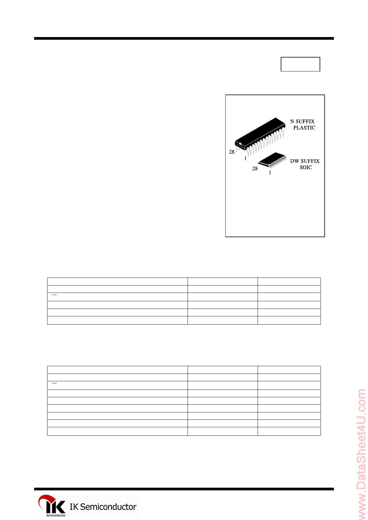
• Standard 28-pin plastic DIP and SOP package.
ORDERING INFORMATION
IL34018N Plastic
IL34018DW SOIC
TA = -25° to 85° C for all packages
www.DataSheet4U.comABSOLUTE MAXIMUM RATINGS (Ta=25℃,Voltages referred to pin 22)
PARAMETER
V+ terminal Voltage (pin 16)
CS (pin 18)
Speaker amplifier Ground(pin 14)
VLC(pin 24)
Storage temperature
VALUE
-1.0 to +12
-1.0 to +12
-1.0 to +3.0
-1.0 to +Vcc
-65 to +150
UNIT
V
V
V
V
℃
RECOMMENDED OPERATION CONDITIONS
PARAMETER
V+ Terminal Voltage (pin 16)
CS (pin 18)
Vcc (pin 20)
VLC(pin 24)
Receive Signal(pin 27)
Microphone Signal(pin 9)
Speaker Amplifier Ground (pin 14)
Ambient Temperature
VALUE
+6.0 to +11
0 to +11
0 to 3.0
0.55VB to VB
0 to 250
0 to 5.0
-10 to +10
-25 to +85
UNIT
V
V
mA
V
mVrms
mVrms
mVdc
℃
1
1 page 
IL34018
ELECTRICAL CHARACTERISTICS (continued)
PARAMETER
TRANSMIT DETECTOR
XDC Voltage
Idle Mode
Tx Mode
CP2 Current Source
Distortion
Rx Mode
RXI to SKO
(pin 27 = 10mVrms,1KHz)
Tx Mode
MCI to TXO
(Pin 9 = 5mVrms,1KHz)
SYMBOL
MIN
VXDC
ICP2
5.0
RXD
TXD
TYP
MAX
UNIT
0
4.0
10 13
Vdc Vdc
A
1.5 %
2.0 %
Note 1:V+=7.5V, CS =0.7V except where noted.
Note 2:Rx mode:pin7=-100 A, pin5=+100 A, except where noted
Tx mode: pin 5,13=-100 A, pin 7=+100 A, pin 11=0V. Idle mode: Pin 5=-100A, pin 7,13=+100 A
Note 3:Current into a pin designed as + ,current out of a pin designed -;
Note 4:Voltage referred to pin 22,Tamb=25 C
TEMPERATURE CHARACTERISTICS (-20 TO +60℃ )
PARAMETER
V+ Supply Current ( V+ 11V,Pin 18 = 0.7V )
V+ Supply Current(V+ 11V,Pin 18 = 1.6V )
VCC Voltage( V+ = 7.5V )
Attenuator Gain ( Max and Min Setting )
Delta RXO,TXO Voltage
Speaker AMP Gain
Microphone AMP Gain
Microphone Amp Input Resistance
Tx-Rx Switching Threshold (20 A)
PIN
16
16
20
4,26
15,19
9,10
9
5,7
TYP CHANGE
-0.2
-0.4
+0.1
+-0.003
+-0.24
+-0.001
+-0.4
+0.4
+-0.2
UNIT
%/ C
%/ C
%/ C
dB/ C
%/ C
dB/ C
dB/ C
%/ C
nA/ C
5
5 Page 
IL34018
SWITCHING TIME
The switching times of the speakerphone circuit
depend not only on the various external components, but
also on the operating condition of the circuit at the time
a change is to take effect. For example, the switching
time from idle to transmit is generally quicker than the
switching time from receive to transmit (or transmit to
receive).
The components which most significantly affect the
timing between the transmit and receive modes are those
at Pins 5 (transmit turn-on), 6 (transmit turn-off), 7
(receive turn-on), and 8 (receive turn-off). These four
timing functions are not independent, but interact since
the Tx-Rx comparator operates on a RELATIVE Tx-Rx
comparison, rather than on absolute values. The
components at Pins 11, 12, 13, and 23 affect the timing
from the transmit to the idle mode. Timing from the idle
mode to transmit mode is relatively quick (due to the
quick charging of the various capacitors), and is not
greatly affected by the component values. Pins 5-8 do
not affect the idle-to-transmit timing since the Tx-Rx
comparator must already be in the transmit mode for this
to occur.
The following table provides a summary of the effect
on the switching time of the various components,
including the volume control :
Additionally, the following should be noted:
1) The RCs at Pins 5 and 7 have a dual function in that
they affect the sensitivity of the respective log
amplifiers, or in other words, how loud the speech must
be in order to gain control of the speakerphone circuit.
2) The RC at Pin 13 also has a dual function in that it
determines the sensitivity of the transmit detector circuit.
3) The volume control affects the switching speed, and
the relative response to transmit signals, in the following
manner: When the circuit is in the receive mode,
reducing the volume control setting increases the signal
at TXO, and consequently the signal to the TLI pin.
Therefore a given signal at TXI will switch the circuit
into the transmit mode quicker at low volume settings.
The photographs of Figures 16 and 17 indicate
experimentally obtained switching response times for the
circuit of Figure 1. In Figure 16, the circuit is provided a
continuous receive signal of 1.1 mVp-p at RXI (trace
#3). A repetitive burst signal of 7.2 mVp-p, lasting 120
11
11 Page | ||
| Páginas | Total 13 Páginas | |
| PDF Descargar | [ Datasheet IL34018.PDF ] | |
Hoja de datos destacado
| Número de pieza | Descripción | Fabricantes |
| IL34018 | Voice Switched Speakerphone Circuit | IK Semiconductor |
| Número de pieza | Descripción | Fabricantes |
| SLA6805M | High Voltage 3 phase Motor Driver IC. |
Sanken |
| SDC1742 | 12- and 14-Bit Hybrid Synchro / Resolver-to-Digital Converters. |
Analog Devices |
|
DataSheet.es es una pagina web que funciona como un repositorio de manuales o hoja de datos de muchos de los productos más populares, |
| DataSheet.es | 2020 | Privacy Policy | Contacto | Buscar |