|
|
|
PDF ICS9250-26 Data sheet ( Hoja de datos )
| Número de pieza | ICS9250-26 | |
| Descripción | Frequency Generator & Integrated Buffers for Celeron & PII/III | |
| Fabricantes | Integrated Circuit Systems | |
| Logotipo | ||
Hay una vista previa y un enlace de descarga de ICS9250-26 (archivo pdf) en la parte inferior de esta página. Total 15 Páginas | ||
|
No Preview Available !
Integrated
Circuit
Systems, Inc.
ICS9250-26
Frequency Generator & Integrated Buffers for Celeron & PII/III™
Recommended Application:
810/810E type chipset. Provides three CPU speeds
(66.6, 100, 133MHz) with SDRAM = 133.3MHz.
Output Features:
• 3 CPU (2.5V) 66.6/133.3MHz (up to 150MHz
achievable through I2C)
• 9 SDRAM (3.3V) @ 133.3MHz (up to 150MHz
achievable through I2C)
• 8 PCI (3.3 V) @33.3MHz
• 2 IOAPIC (2.5V) @ 33.3 MHz
• 2 Hublink clocks (3.3 V) @ 66.6 MHz
• 2 USB (3.3V) @ 48 MHz ( Non spread spectrum)
• 1 REF (3.3V) @ 14.318 MHz
Features:
• Supports spread spectrum modulation ,
down spread 0 to -0.5% and ± 0.25% center spread.
• I2C support for power management
• Efficient power management scheme through PD#
• Uses external 14.138 MHz crystal
• Alternate frequency selections available through I2C
control.
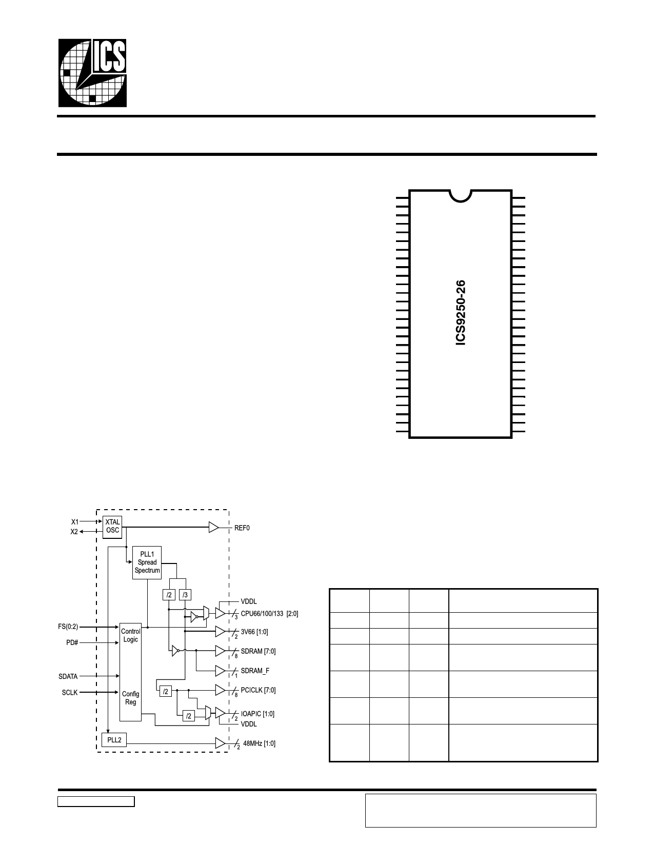
Block Diagram
Pin Configuration
*FS2//REF0
VDD0
X1
X2
GND0
GND1
3V66-0
3V66-1
VDD1
VDD2
PCICLK0
PCICLK1
PCICLK2
GND2
PCICLK3
PCICLK4
GND2
PCICLK5
PCICLK6
PCICLK7
VDD2
VDD3
GND3
GND4
48MHz_0
48MHz_1
VDD4
FS0
1
2
3
4
5
6
7
8
9
10
11
12
13
14
15
16
17
18
19
20
21
22
23
24
25
26
27
28
56 GNDL1
55 IOAPIC0
54 IOAPIC1
53 VDDL1
52 CPUCLK0
51 VDDL0
50 CPUCLK1
49 CPUCLK2
48 GNDL0
47 GND5
46 SDRAM0
45 SDRAM1
44 VDD5
43 SDRAM2
42 SDRAM3
41 GND5
40 SDRAM4
39 SDRAM5
38 VDD5
37 SDRAM6
36 SDRAM7
35 GND5
34 SDRAM_F
33 VDD5
32 PD#
31 SCLK
30 SDATA
29 FS1
56-Pin 300mil SSOP
* This input has a 120KΩ pull-down to GND.
9250-26 Rev B 01/19/01
Third party brands and names are the property of their respective owners.
Functionality
FS2 FS1 FS0
Function
X 0 0 Tristate
X0
1 Test
0
1
0
Active CPU = 66MHz
SDRAM = 100MHz
0
1
1
Active CPU = 100MHz
SDRAM = 100MHz
1
1
1
Active CPU = 133MHz
SDRAM = 100MHz
(Special Condition)
1 1 0 Active CPU = 133MHz
SDRAM = 133MHz
ICS reserves the right to make changes in the device data identified in
this publication without further notice. ICS advises its customers to
obtain the latest version of all device data to verify that any
information being relied upon by the customer is current and accurate.
1 page 
ICS9250-26
Byte 5: ICS Reserved Functionality and frequency select register (Default as noted in PWD)
Bit
Bit7
Bit6
Bit5
Bit
(3,0)
Bit4
Bit2
Bit1
Desctiption
ICS RESERVED BIT (Needs to be 0 clock to operate normal)
ICS RESERVED BIT (Needs to be 0 clock to operate normal)
ICS RESERVED BIT (Needs to be 0 clock to operate normal)
FS2
(HW)
Bit (3,0)
FS0 SEL1
(HW) (Bit3)
CPUCLK SDRAM 3V66
SEL0
MHz
MHz MHz
(Bit0)
0 0 0 0 66.67 100.00 66.60
0 0 0 1 70.00 105.00 70.00
0 0 1 0 72.67 109.00 72.67
0 0 1 1 74.67 112.00 74.66
0 1 0 0 100.00 100.00 66.60
0 1 0 1 105.00 105.00 70.00
0 1 1 0 109.00 109.00 72.67
0 1 1 1 112.01 112.00 74.66
1 0 0 0 133.34 133.34 88.66
1 0 0 1 140.00 105.00 70.00
10
1 0 120.00 90.00 60.00
1 0 1 1 124.00 124.00 82.66
1 1 0 0 133.34 100.00 66.60
1 1 0 1 150.00 150.00 75.00
1 1 1 0 140.00 140.00 70.00
1 1 1 1 132.99 132.99 66.60
0 = Down Spread Spread Spectrum 0 to -.5%
1 = Center Spread Spread Spectrum ± .25%
Not used (Needs to be 1 for normal clock operation)
Not used (Needs to be 1 for normal clock operation)
PCICLK
MHz
33.30
35.00
36.33
37.33
33.30
35.00
36.33
37.33
44.33
35.00
30.00
41.33
33.30
37.50
35.00
33.30
PWD
0
0
0
XXXX
Note 1
0
1
1
Note1: Default at power-up will be for Bit 3 and Bit 0 to be 00, with external hardware selection of FS0, FS2
defining specific frequency.
5
5 Page 
ICS9250-26
Electrical Characteristics - PCI
TA = 0 - 70C; VDD = 3.3 V +/-5%; CL = 10-30 pF (unless otherwise specified)
PARAMETER
SYMBOL
CONDITIONS
Output Impedance
Output Impedance
Output High Voltage
Output Low Voltage
Output High Current
RDSP1B1
RDSN1B1
VOH1
VOL1
IOH1
VO = VDD*(0.5)
VO = VDD*(0.5)
IOH = -1 mA
IOL = 1 mA
VOH @ MIN = 1.0 V
VOH @ MAX = 3.135 V
Output Low Current
Rise Time1
Fall Time1
Duty Cycle1
Skew window1
Jitter, Cycle-to-cycle1
IOL1
tr1
tf1
dt1
tsk1
tjcyc-cyc1
VOL @ MIN = 1.95 V
VOL @ MAX = 0.4 V
VOL = 0.4 V, VOH = 2.4 V
VOH = 2.4 V, VOL = 0.4 V
VT = 1.5 V
VT = 1.5 V
VT = 1.5 V
1Guaranteed by design, not 100% tested in production.
MIN TYP MAX UNITS
12 15 55 Ω
12 15 55 Ω
2.4 V
0.55 V
-33 -106
mA
-14 -33
30 94
mA
29 38
0.4 1.3 2 ns
0.4 1.4 2 ns
45 51 55 %
250 500 ps
150 500 ps
Electrical Characteristics - REF, 48M Hz_0 (Pin 25)
TA = 0 - 70C; VDD = 3.3 V +/-5%; CL = 10-20 pF (unles s otherwis e s pecified)
PA RA M ETER
SYM BOL
CONDITIONS
M IN
Output Impedance
Output Impedance
Output High Voltage
R
DSP5
1
B
R
DSN5
1
B
VO H 15
VO = VDD*(0.5)
VO = VDD*(0.5)
IOH = -1 mA
20
20
2.4
Output Low Voltage
VO L5
IOL = 1 mA
Output High Current
IO H 5
VO H @ MIN = 1.0 V
VOH @ MAX = 3.135 V
-29
Output Low Current
Ris e Time1
Fall Time1
Duty Cycle1
Jitter, Cycle-to-cycle1
Jitter, Cycle-to-cycle1
IO L5
tr5
tf5
dt5
tjcyc-cyc5
tjcyc-cyc5
VOL @ MIN = 1.95 V
VO L @ MA X = 0.4 V
VOL = 0.4 V, VOH = 2.4 V
VOH = 2.4 V, VOL = 0.4 V
VT = 1.5 V
VT = 1.5 V, Fixed clocks
VT = 1.5 V, Ref clocks
29
0.4
0.4
45
1Guaranteed by des ign, not 100% tes ted in production.
TYP M A X UNITS
29 60 Ω
27 60 Ω
V
0.55 V
-54
mA
-11 -23
54
mA
16 27
1.1 4 ns
1.6 4 ns
53 55 %
130 500 ps
650 1000 ps
11
11 Page | ||
| Páginas | Total 15 Páginas | |
| PDF Descargar | [ Datasheet ICS9250-26.PDF ] | |
Hoja de datos destacado
| Número de pieza | Descripción | Fabricantes |
| ICS9250-22 | Frequency Generator & Integrated Buffers for Celeron & PII/III | Integrated Circuit Systems |
| ICS9250-23 | Frequency Generator & Integrated Buffers for Celeron & PII/III | Integrated Circuit Systems |
| ICS9250-25 | Frequency Generator & Integrated Buffers for Celeron & PII/III | Integrated Circuit Systems |
| ICS9250-26 | Frequency Generator & Integrated Buffers for Celeron & PII/III | Integrated Circuit Systems |
| Número de pieza | Descripción | Fabricantes |
| SLA6805M | High Voltage 3 phase Motor Driver IC. |
Sanken |
| SDC1742 | 12- and 14-Bit Hybrid Synchro / Resolver-to-Digital Converters. |
Analog Devices |
|
DataSheet.es es una pagina web que funciona como un repositorio de manuales o hoja de datos de muchos de los productos más populares, |
| DataSheet.es | 2020 | Privacy Policy | Contacto | Buscar |