|
|
|
PDF ICS9250-27 Data sheet ( Hoja de datos )
| Número de pieza | ICS9250-27 | |
| Descripción | Frequency Generator & Integrated Buffers for Celeron & PII/III | |
| Fabricantes | Integrated Circuit Systems | |
| Logotipo | ||
Hay una vista previa y un enlace de descarga de ICS9250-27 (archivo pdf) en la parte inferior de esta página. Total 14 Páginas | ||
|
No Preview Available !
Integrated
Circuit
Systems, Inc.
ICS9250-27
Frequency Generator & Integrated Buffers for Celeron & PII/III™
Recommended Application:
810/810E and 815 type chipset.
Output Features:
• 3 CPU (2.5V) (up to 133MHz achievable through I2C)
• 9 SDRAM (3.3V) (up to 133MHz achievable
through I2C)
• 7 PCI (3.3 V) @33.3MHz
• 2 IOAPIC (2.5V) @ 33.3 MHz
• 3 Hublink clocks (3.3 V) @ 66.6 MHz
• 2 (3.3V) @ 48 MHz (Non spread spectrum)
• 1 REF (3.3V) @ 14.318 MHz
Features:
• Supports spread spectrum modulation,
0 to -0.5% down spread.
• I2C support for power management
• Efficient power management scheme through PD#
• Uses external 14.138 MHz crystal
• Alternate frequency selections available through I2C
control.
*FS2//REF0
VDD
X1
X2
GND
GND
3V66-0
3V66-1
3V66-2
VDD
VDD
PCICLK_F
PCICLK0
GND
PCICLK1
PCICLK2
GND
PCICLK3
PCICLK4
PCICLK5
VDD
VDD
GND
GND
48MHz_0
48MHz_1
VDD
FS0
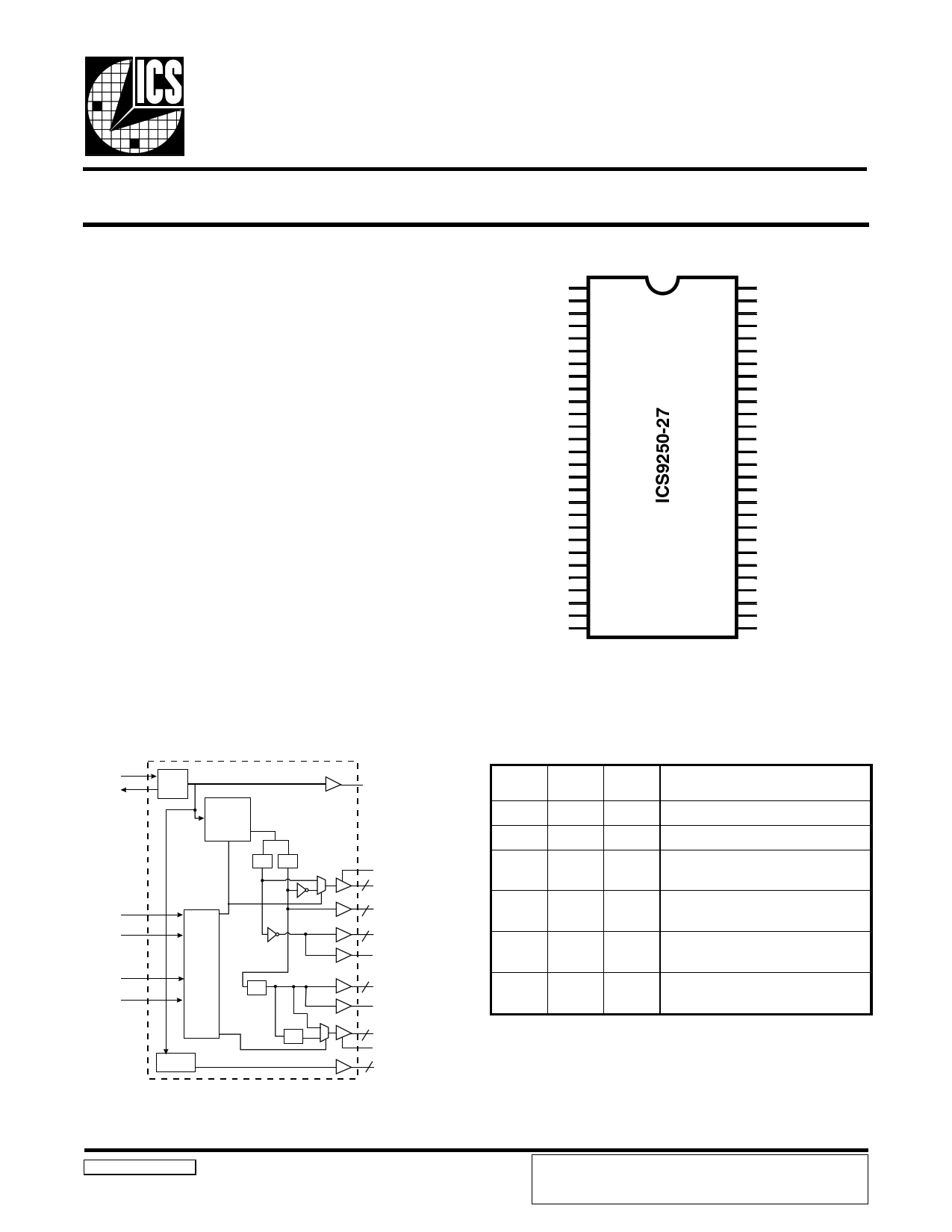
Pin Configuration
1 56 GND
2 55 IOAPIC0
3 54 IOAPIC1
4 53 VDDL
5 52 CPUCLK0
6 51 VDDL0
7 50 CPUCLK1
8 49 CPUCLK2
9 48 GNDL
10 47 GND
11 46 SDRAM0
12 45 SDRAM1
13 44 VDD
14 43 SDRAM2
15 42 SDRAM3
16 41 GND
17 40 SDRAM4
18 39 SDRAM5
19 38 VDD
20 37 SDRAM6
21 36 SDRAM7
22 35 GND
23 34 SDRAM_F
24 33 VDD
25 32 PD#
26 31 SCLK
27 30 SDATA
28 29 FS1
Block Diagram
56-Pin 300mil SSOP
* This input has a 50KΩ pull-down to GND.
Functionality
X1 XTAL
X2 OSC
PLL1
Spread
Spectrum
/2 /3
FS (2:0)
PD#
SDATA
SCLK
Control
Logic
Config
Reg
PLL2
/2
/2
REF0
VDDL
3 CPU66/100/133 (2:0)
3V66 (2:0)
3
SDRAM (7:0)
8
SDRAM_F
PCICLK (5:0)
6
PCICLK_F
IOAPIC (1:0)
2
VDDL
2 48MHz (1:0)
FS2 FS1 FS0
Function
X 0 0 Tristate
X0
1 Test
0
1
0
Active CPU = 66MHz
SDRAM = 100MHz
0
1
1
Active CPU = 100MHz
SDRAM = 100MHz
1
1
0
Active CPU = 133MHz
SDRAM = 133MHz
1
1
1
Active CPU = 133MHz
SDRAM = 100MHz
Power Groups
AVDD = Pin 22 Analog power for PLL
AGND = Pin 23 Analog ground
VDD48 = Pin 27 Analog power for 48MHz PLL
GND = Pin 24 Analog ground for 48MHz PLL
9250-27 Rev B 02/15/01
Third party brands and names are the property of their respective owners.
ICS reserves the right to make changes in the device data identified in
this publication without further notice. ICS advises its customers to
obtain the latest version of all device data to verify that any
information being relied upon by the customer is current and accurate.
1 page 
ICS9250-27
Byte 2: Control Register
(1 = enable, 0 = disable)
Bit Pin#
Name
Bit 7 9 3V66-2 (AGP)
Bit 6 20 PCICLK5
Bit 5 19 PCICLK4
Bit 4 18 PCICLK3
Bit 3 16 PCICLK2
Bit 2 15 PCICLK1
Bit 1 13 PCICLK0
Bit 0 - Undefined bit
PWD Description
1 (Active/Inactive)
1 (Active/Inactive)
1 (Active/Inactive)
1 (Active/Inactive)
1 (Active/Inactive)
1 (Active/Inactive)
1 (Active/Inactive)
X (Active/Inactive)
Notes:
1. Inactive means outputs are held LOW and are disabled from switching. These outputs are designed to be
configured at power-on and are not expected to be configured during the normal modes of operation.
2. PWD = Power on Default
3. Undefined bit can be wirtten with either a "1" or "0".
Byte 3: ICS Reserved Functionality and frequency select register (Default as noted in PWD)
Bit
Bit7
Bit6
Bit5
Bit4
Bit3
Bit2
Bit1
Bit 0
ICS Reserved bit (Note 2)
ICS Reserved bit (Note 2)
ICS Reserved bit (Note 2)
ICS Reserved bit (Note 2)
ICS Reserved bit (Note 2)
Undefined bit (Note 3)
Undefined bit (Note 3)
Bit 0 FS0
FS1
000
0 10
00 1
0 11
10 0
1 10
10 1
111
Desctiption
CPUCLK SDRAM
MHz
MHz
66.66 100.0
100.0 100.0
133.32 133.32
133.32 100.0
66.66 100.0
100.0 100.0
133.32 133.32
133.32 133.32
3V66
MHz
66.66
66.66
66.66
66.66
66.66
66.66
66.66
66.66
PCICLK IOAPIC
MHz MHz
33.33 33.33
33.33 33.33
33.33 33.33
33.33 33.33
33.33 33.33
33.33 33.33
33.33 33.33
33.33 33.33
PWD
0
0
0
0
0
X
X
0
Note 1
Note 1: For system operation, the BSEL lines of the CPU will program FS0, FS2 for the appropriate CPU speed, always with
SDRAM = 100MHz. After BIOS verifies the SDRAM is PC133 speed, then bit 0 can be written from the default 0 to
1 to change the SDRAM output frequency from 100MHz to 133MHz. This will only change if the CPU is at the
133MHz FSB speed as shown in this table. The CPU, 3v66, PCI, and IOAPIC clocks will be glitch free during this
transition, and only SDRAM will change.
Note 2: "ICS RESERVED BITS" must be writtern as "O".
Note3: Undefined bits can be written either as "1 or 0"
5
5 Page 
ICS9250-27
Electrical Characteristics - 48MHz_1 (Pin 26)
TA = 0 - 70C; VDD = 3.3 V +/-5%; CL = 10-15 pF (unless otherwise specified)
PARAMETER
SYMBOL
CONDITIONS
Output Impedance
Output Impedance
Output High Voltage
Output Low Voltage
Output High Current
Output Low Current
Rise Time1
Fall Time1
Duty Cycle1
Skew
Jitter, Cycle-to-cycle1
RDSP31
RDSN31
VOH3
VOL3
IOH3
IOL3
tr3
tf3
dt3
tsk3
tjcyc-cyc3B
VO = VDD*(0.5)
VO = VDD*(0.5)
IOH = -1 mA
IOL = 1 mA
VOH @ MIN = 2.0 V
VOH @ MAX = 3.135 V
VOL @ MIN = 1.0 V
VOL @ MAX = 0.4 V
VOL = 0.4 V, VOH = 2.4 V
VOH = 2.4 V, VOL = 0.4 V
VT = 1.5 V
VT = 1.5 V
VT = 1.5 V
1Guaranteed by design, not 100% tested in production.
MIN TYP MAX UNITS
10 16.7 24
Ω
10 18.4 24
Ω
2.4 V
0.55 V
-54
-82
-20
-46 mA
54
95
28
53 mA
0.4 1.1 1.6 ns
0.4 1.1 1.6 ns
45 51 55 %
116 250 ps
196 500 ps
11
11 Page | ||
| Páginas | Total 14 Páginas | |
| PDF Descargar | [ Datasheet ICS9250-27.PDF ] | |
Hoja de datos destacado
| Número de pieza | Descripción | Fabricantes |
| ICS9250-22 | Frequency Generator & Integrated Buffers for Celeron & PII/III | Integrated Circuit Systems |
| ICS9250-23 | Frequency Generator & Integrated Buffers for Celeron & PII/III | Integrated Circuit Systems |
| ICS9250-25 | Frequency Generator & Integrated Buffers for Celeron & PII/III | Integrated Circuit Systems |
| ICS9250-26 | Frequency Generator & Integrated Buffers for Celeron & PII/III | Integrated Circuit Systems |
| Número de pieza | Descripción | Fabricantes |
| SLA6805M | High Voltage 3 phase Motor Driver IC. |
Sanken |
| SDC1742 | 12- and 14-Bit Hybrid Synchro / Resolver-to-Digital Converters. |
Analog Devices |
|
DataSheet.es es una pagina web que funciona como un repositorio de manuales o hoja de datos de muchos de los productos más populares, |
| DataSheet.es | 2020 | Privacy Policy | Contacto | Buscar |