|
|
|
PDF IN74ACT299 Data sheet ( Hoja de datos )
| Número de pieza | IN74ACT299 | |
| Descripción | 8-Bit Universal Shift/Storage Register | |
| Fabricantes | IK Semiconductor | |
| Logotipo | ||
Hay una vista previa y un enlace de descarga de IN74ACT299 (archivo pdf) en la parte inferior de esta página. Total 8 Páginas | ||
|
No Preview Available !
TECHNICAL DATA
8-Bit Bidirectional Universal
Shift Register with Parallel I/O
High-Speed Silicon-Gate CMOS
IN74ACT299
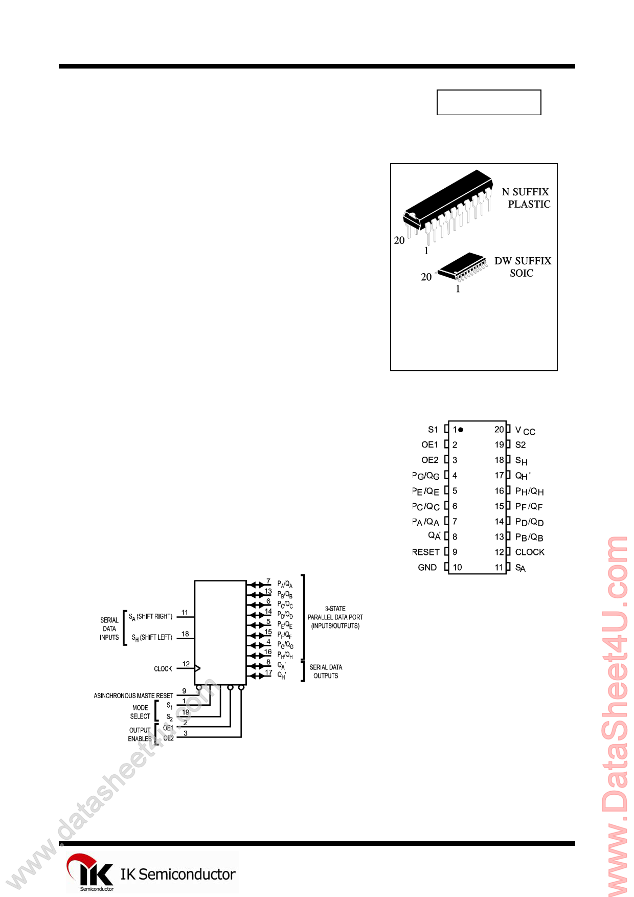
The IN74ACT299 is identical in pinout to the LS/ALS299,
HC/HCT299. The IN74ACT299 may be used as a level converter for
interfacing TTL or NMOS outputs to High Speed CMOS inputs.
The IN74ACT299 features a multiplexed parallel input/output data
port to achieve full 8-bit handling in a 20 pin package. Due to the large
output drive capability and the 3-state feature, this device is ideally suited
for interface with bus lines in a bus-oriented system.
Two Mode-Select inputs and two Output Enable inputs are used to
choose the mode of operation as listed in the Function Table.
Synchronous parallel loading is accomplished by taking both Mode-
Select lines, S1 and S2, high. This places the outputs in the high-
impedance state, which permits data applied to the data port to be clocked
into the register. Reading out of the register can be accomplished when
the outputs are enabled. The active-low asynchronous Reset overrides all
other inputs.
• TTL/NMOS Compatible Input Levels
• Outputs Directly Interface to CMOS, NMOS, and TTL
• Operating Voltage Range: 4.5 to 5.5 V
• Low Input Current: 1.0 µA; 0.1 µA @ 25°C
• Outputs Source/Sink 24 mA
ORDERING INFORMATION
IN74ACT299N Plastic
IN74ACT299DW SOIC
TA = -40° to 85° C for all packages
PIN ASSIGNMENT
LOGIC DIAGRAM
www.datasheet4u.coPPImNIN1020==GVNCCD
1
1 page 
IN74ACT299
FUNCTION TABLE
Inputs
Response
Mode
Reset
Mode
Select
S2 S1
Output
Enables
OE1 OE2
Clock
Serial PA/ PB/ PC/ PD/ PE/ PF/ PG/ PH/ QA’ QH’
Inputs QA QB QC QD QE QF QG QH
DA DH
Reset L X L L L X X X L L L L L L L L L L
L L X L L X X XLLLLLLL L L L
Shift
Right
L HH X
H LH H
X
X
X XX
QA through QH=Z
LL
DX
Shift Right: QA through QH=Z;
DA FA; FA FB; etc
D QG
H LH X H
DX
Shift Right: QA through QH=Z;
DA FA; FA FB; etc
D QG
H LH L L
DX
Shift Right: DA FA =QA;
FA FB =QB; etc
D QG
Shift
Left
H HL H
X
H HL X H
H HL L L
Parallel H H H X
Load
X
XD
XD
XD
XX
Shift Left: QA through QH=Z;
DH FH; FH FG; etc
Shift Left: QA through QH=Z;
DH FH; FH FG; etc
Shift Left: DH FH =QH;
FH FG =QG; etc
Parallel Load:PN FN
QB D
QB D
QB D
PA PH
Hold
H LL H
H LL X
X
H
X X X Hold: QA through QH=Z; FN=FN PA PH
X X X Hold: QA through QH=Z; FN=FN PA PH
H L L L L X XX
Hold: QN =QH
PA PH
Z = high impedance
D = data on serial input
F = flip-flop (see Logic Diagram)
When one or both output controls are high the eight input/output terminals are disabled to the high-
impedance state; however, sequential operation or clearing of the register is not affected.
5
5 Page | ||
| Páginas | Total 8 Páginas | |
| PDF Descargar | [ Datasheet IN74ACT299.PDF ] | |
Hoja de datos destacado
| Número de pieza | Descripción | Fabricantes |
| IN74ACT299 | 8-Bit Universal Shift/Storage Register | IK Semiconductor |
| Número de pieza | Descripción | Fabricantes |
| SLA6805M | High Voltage 3 phase Motor Driver IC. |
Sanken |
| SDC1742 | 12- and 14-Bit Hybrid Synchro / Resolver-to-Digital Converters. |
Analog Devices |
|
DataSheet.es es una pagina web que funciona como un repositorio de manuales o hoja de datos de muchos de los productos más populares, |
| DataSheet.es | 2020 | Privacy Policy | Contacto | Buscar |