|
|
|
PDF IN74ACT652 Data sheet ( Hoja de datos )
| Número de pieza | IN74ACT652 | |
| Descripción | Octal Bus Transceiver/Register | |
| Fabricantes | IK Semiconductor | |
| Logotipo | ||
Hay una vista previa y un enlace de descarga de IN74ACT652 (archivo pdf) en la parte inferior de esta página. Total 9 Páginas | ||
|
No Preview Available !
TECHNICAL DATA
Octal 3-State Bus Transceivers
and D Flip-Flops
High-Speed Silicon-Gate CMOS
IN74ACT652
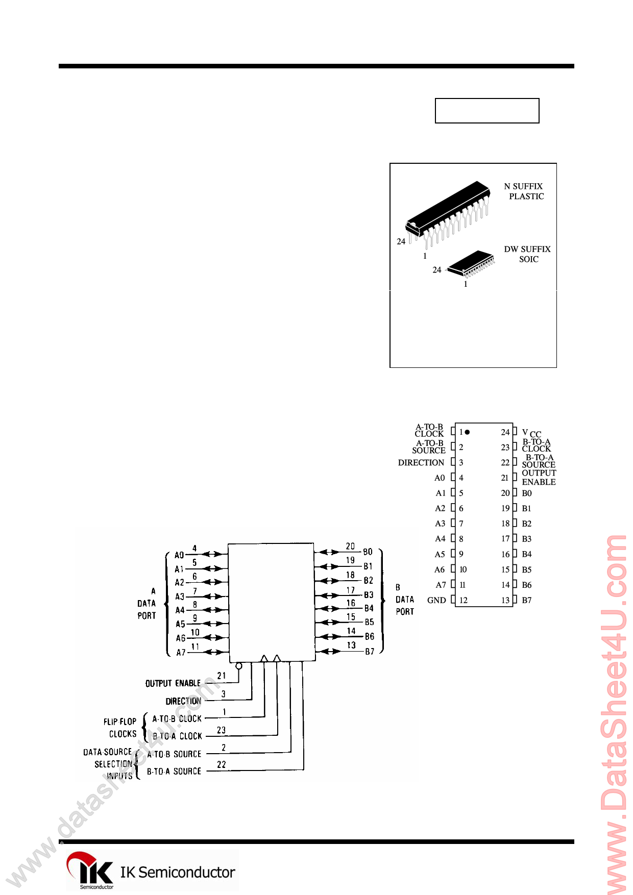
The IN74ACT652 is identical in pinout to the LS/ALS652,
HC/HCT652. The IN74ACT652 may be used as a level converter for
interfacing TTL or NMOS outputs to High Speed CMOS inputs.
These devices consists of bus transceiver circuits, D-type flip-flop,
and control circuitry arranged for multiplex transmission of data directly
from the data bus or from the internal storage registers. Direction and
Output Enable are provided to select the read-time or stored data function.
Data on the A or B Data bus, or both, can be stored in the internal D flip-
flops by low-to-high transitions at the appropriate clock pins (A-to-B
Clock or B-to-A Clock) regardless of the select or enable or enable
control pins. When A-to-B Source and B-to-A Source are in the real-time
transfer mode, it is also possible to store data without using the internal
D-type flip-flops by simultaneously enabling Direction and Output
Enable. In this configuration each output reinforces its input. Thus, when
all other data sources to the two sets of bus lines are at high impedance,
each set of bus lines will remain at its last state.
The IN74ACT652 has noninverted outputs.
• TTL/NMOS Compatible Input Levels
• Outputs Directly Interface to CMOS, NMOS, and TTL
• Operating Voltage Range: 4.5 to 5.5 V
• Low Input Current: 1.0 µA; 0.1 µA @ 25°C
• Outputs Source/Sink 24 mA
ORDERING INFORMATION
IN74ACT652N Plastic
IN74ACT652DW SOIC
TA = -40° to 85° C for all packages
PIN ASSIGNMENT
LOGIC DIAGRAM
www.datasheet4u.comPPININ1224==GVNCCD
1
1 page 
IN74ACT652
TIMING REQUIREMENTS (CL=50pF,Input tr=tf=3.0 ns)
Symbol
Parameter
VCC*
V
tsu Minimum Setup Time, A or B Data Port to A- 5.0
to-B Clock or B-to-A Clock (Figure 7)
th Minimum Hold Time, A-to-B Clock or
5.0
B-to-A Clock to A or B Data Port (Figure 7)
tw Minimum Pulse Width, A-to-B Clock or
B-to-A Clock (Figure 7)
5.0
Guaranteed Limits
25 °C
-40°C to
85°C
7.0 8.0
2.5 2.5
6.0 7.0
Unit
ns
ns
ns
TIMING DIAGRAM
5
5 Page | ||
| Páginas | Total 9 Páginas | |
| PDF Descargar | [ Datasheet IN74ACT652.PDF ] | |
Hoja de datos destacado
| Número de pieza | Descripción | Fabricantes |
| IN74ACT651 | Octal Bus Transceiver/Register | IK Semiconductor |
| IN74ACT652 | Octal Bus Transceiver/Register | IK Semiconductor |
| Número de pieza | Descripción | Fabricantes |
| SLA6805M | High Voltage 3 phase Motor Driver IC. |
Sanken |
| SDC1742 | 12- and 14-Bit Hybrid Synchro / Resolver-to-Digital Converters. |
Analog Devices |
|
DataSheet.es es una pagina web que funciona como un repositorio de manuales o hoja de datos de muchos de los productos más populares, |
| DataSheet.es | 2020 | Privacy Policy | Contacto | Buscar |