|
|
PDF A40MX02 Data sheet ( Hoja de datos )
| Número de pieza | A40MX02 | |
| Descripción | 40MX and 42MX FPGA Families | |
| Fabricantes | Actel Corporation | |
| Logotipo |  |
|
Hay una vista previa y un enlace de descarga de A40MX02 (archivo pdf) en la parte inferior de esta página. Total 70 Páginas | ||
|
No Preview Available !
v5.0
40MX and 42MX FPGA Families
Features
High Capacity
• Single-Chip ASIC Alternative
• 3,000 to 54,000 System Gates
• Up to 2.5 kbits Configurable Dual-Port SRAM
• Fast Wide-Decode Circuitry
• Up to 202 User-Programmable I/O Pins
High Performance
• 5.6 ns Clock-to-Out
• 250 MHz Performance
• 5 ns Dual-Port SRAM Access
• 100 MHz FIFOs
• 7.5 ns 35-Bit Address Decode
HiRel Features
• Commercial, Industrial, and Military Temperature Plastic
Packages
Product Profile
Device
A40MX02
Capacity
System Gates
SRAM Bits
3,000
N/A
Logic Modules
Sequential
Combinatorial
Decode
Clock-to-Out
—
295
—
9.5 ns
SRAM Modules
(64x4 or 32x8)
N/A
Dedicated Flip-Flops
—
Maximum Flip-Flops
mClocks
oUser I/O (Maximum)
.cPCI
uBoundary Scan Test (BST)
t4Packages (by pin count)
ePLCC
ePQFP
hVQFP
sTQFP
taCQFP
PBGA
147
1
57
No
No
44, 68
100
80
—
—
—
w.daFebruary 2001
ww © 2001 Actel Corporation
A40MX04
6,000
N/A
—
547
—
9.5 ns
N/A
—
273
1
69
No
No
44, 68, 84
100
80
—
—
—
• Commercial, Military Temperature and MIL-STD-883
Ceramic Packages
• QML Certification
• Ceramic Devices Available to DSCC SMD
Ease of Integration
• Mixed Voltage Operation (5.0V or 3.3V I/O)
• Synthesis-Friendly Architecture to Support ASIC Design
Methodologies
• Up to 100% Resource Utilization and 100% Pin Fixing
• Deterministic, User-Controllable Timing
• Unique In-System Diagnostic and Verification Capability
with Silicon Explorer II
• Low Power Consumption
• IEEE Standard 1149.1 (JTAG) Boundary Scan Testing
• 5.0V and 3.3V Programmable PCI-Compliant I/O
A42MX09
14,000
N/A
348
336
N/A
5.6 ns
N/A
348
516
2
104
No
No
84
100, 160
100
176
—
—
A42MX16
24,000
N/A
624
608
N/A
6.1 ns
N/A
624
928
2
140
No
No
84
100, 160, 208
100
176
—
—
A42MX24
36,000
N/A
954
912
24
6.1 ns
N/A
954
1,410
2
176
Yes
Yes
84
160, 208
—
176
—
—
A42MX36
54,000
2,560
1,230
1,184
24
6.3 ns
10
1,230
1,822
6
202
Yes
Yes
—
208, 240
—
—
208, 256
272
1
1 page 
40MX and 42MX FPGA Families
Power Requirements
40MX
The 40MX FPGAs will operate in 5.0V-only systems or
3.3V-only systems.
VCC Input Output
5.0V 5.0V 5.0V
3.3V 3.3V 3.3V
42MX
The 42MX FPGAs will operate in 5.0V-only systems,
3.3V-only systems, or mixed 5.0V/3.3V systems.
VCCA VCCI Input
5.0V 5.0V 5.0V
Output
5.0V
3.3V 3.3V 3.3V
3.3V
5.0V 3.3V 3.3V, 5.0V 3.3V
Mixed Voltage Power Up and Power
Down
When powering up the device in the mixed voltage mode
(VCCA = 5.0V and VCCI = 3.3V), VCCA must be greater than or
equal to VCCI throughout the power-up sequence. If VCCI is
0.5V greater than VCCA when both are above 1.5V, then the
I/Os’ input protection junction on the I/Os will be forward
biased, causing them to draw large amounts of current.
When VCCA and VCCI are in the 1.5V to 2.0V region and VCCI
is greater than VCCA, all I/Os would momentarily behave as
outputs that are in a logical high state, and ICC rises to high
levels. For power down, any sequence with VCCA and VCCI
can be implemented.
Low Power Mode
The 42MX devices have a power-saving feature enabled by a
special Low Power pin (LP). In this mode, the device
consumes very minimal power, with standby current as low
as 15µA (see “Electrical Specifications” on page 13 and 14).
All µ I/Os are tristated, all input buffers are turned off, and
the core of the device is turned off. Since the core is turned
off, the state of the registers and the contents of the SRAM
are lost. The device enters low power mode 800ns after the
LP pin is set High. It will resume normal operation 200µs
after the LP pin is driven to a logic Low.
MX Architectural Overview
The 40MX and 42MX devices are composed of fine-grained
building blocks that enable fast, efficient logic designs. All
devices within these families are composed of logic
modules, I/O modules, routing resources, and clock
networks, which are the building blocks for designing fast
logic designs. In addition, the A42MX36 device contains
embedded dual-port SRAM and wide decode modules. The
dual-port SRAM modules are optimized for high-speed
datapath functions such as FIFOs, LIFOs, and scratchpad
memory. The “Product Profile” on page 1 lists the specific
logic resources contained within each device.
Logic Modules
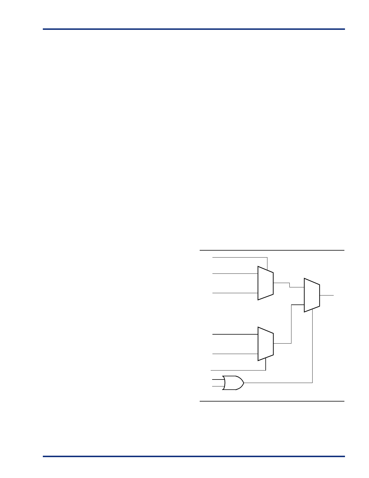
The 40MX logic module is an eight-input, one-output logic
circuit designed to implement a wide range of logic
functions with efficient use of interconnect routing
resources (Figure 1).
The logic module can implement the four basic logic
functions (NAND, AND, OR, and NOR) in gates of two, three,
or four inputs. Each function may have many versions with
different combinations of active LOW inputs. The logic
module can also implement a variety of D-latches,
exclusivity functions, AND-ORs, and OR-ANDs. No dedicated
hard-wired latches or flip-flops are required in the array,
since latches and flip-flops can be constructed from logic
modules wherever needed in the application.
Figure 1 • 40MX Logic Module
v5.0
5
5 Page 
40MX and 42MX FPGA Families
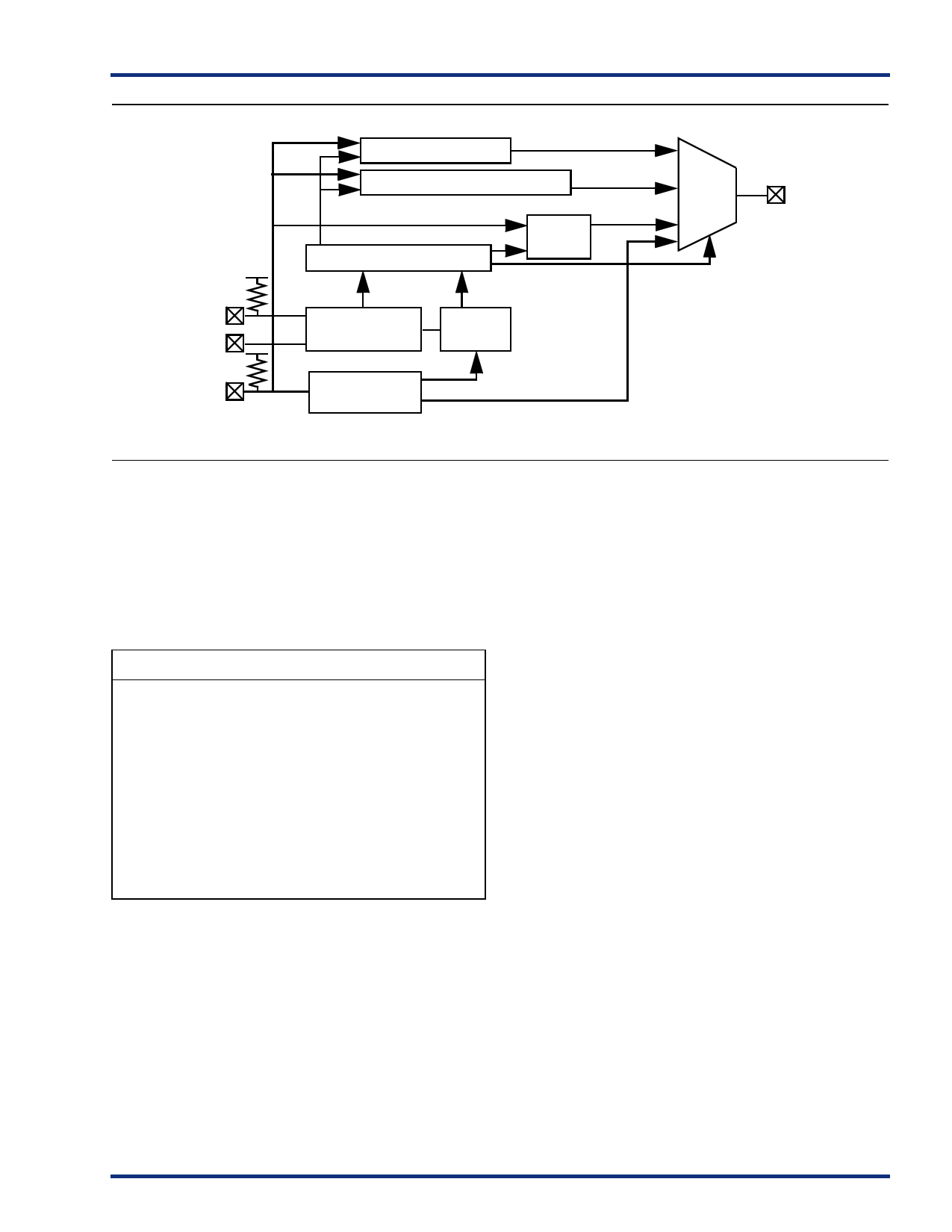
JTAG
TMS
TCK
JTAG
TDI
JPROBE Register
Boundary Scan Register
Control Logic
Bypass
Register
TAP Controller
Instruction
Decode
Instruction
Register
Output
MUX
TDO
Figure 11 • 42MX IEEE 1149.1 Boundary Scan Circuitry
When a device is operating in BST mode, four I/O pins are
used for the TDI, TDO, TMS, and TCK signals. An active
reset (nTRST) pin is not supported; however, the 42MX
device contain power-on circuitry that resets the boundary
scan circuitry upon power-up. Table 1 summarizes the
functions of the IEEE 1149.1 BST signals.
Table 1 • IEEE 1149.1 BST Signals
Signal Name
Function
TDI
TDO
TMS
TCK
Test Data In
Test Data
Out
Test Mode
Select
Test Clock
Serial data input for BST
instructions and data. Data is
shifted in on the rising edge of
TCK.
Serial data output for BST
instructions and test data.
Serial data input for BST mode.
Data is shifted in on the rising
edge of TCK.
Clock signal to shift the BST
data into the device.
JTAG
All SX-A devices are IEEE 1149.1 (JTAG) compliant. SX-A
devices offer superior diagnostic and testing capabilities by
providing JTAG and probing capabilites. These functions
are controlled through the special JTAG pins in conjunction
with the program fuse.
JTAG fuse programmed:
• TCK must be terminated—logical high or low doesn’t
matter (to avoid floating input)
• TDI, TMS may float or at logical high (internal pull-up is
present)
• TDO may float or connect to TDI of another device (it’s an
output)
JTAG fuse not programmed:
• TCK, TDI, TDO, TMS are user I/O. If not used, they will be
configured as tristated output.
BST Instructions
Boundary scan testing within the 42MX devices is controlled
by a Test Access Port (TAP) state machine. The TAP
controller drives the three-bit instruction register, a bypass
register, and the boundary scan data registers within the
device. The TAP controller uses the TMS signal to control
the testing of the device. The BST mode is determined by
the bitstream entered on the TMS pin. Table 2 describes the
test instructions supported by the 42MX devices.
Reset
The TMS pin is equipped with an internal pull-up resistor.
This allows the TAP controller to remain in or return to the
Test-Logic-Reset state when there is no input or when a
logical 1 is on the TMS pin. To reset the controller, TMS
must be HIGH for at least five TCK cycles.
v5.0
11
11 Page | ||
| Páginas | Total 70 Páginas | |
| PDF Descargar | [ Datasheet A40MX02.PDF ] | |
Hoja de datos destacado
| Número de pieza | Descripción | Fabricantes |
| A40MX02 | 40MX and 42MX FPGA Families | Actel Corporation |
| A40MX04 | 40MX and 42MX FPGA Families | Actel Corporation |
| Número de pieza | Descripción | Fabricantes |
| SLA6805M | High Voltage 3 phase Motor Driver IC. |
Sanken |
| SDC1742 | 12- and 14-Bit Hybrid Synchro / Resolver-to-Digital Converters. |
Analog Devices |
|
DataSheet.es es una pagina web que funciona como un repositorio de manuales o hoja de datos de muchos de los productos más populares, |
| DataSheet.es | 2020 | Privacy Policy | Contacto | Buscar |
