|
|
|
PDF ICS1524 Data sheet ( Hoja de datos )
| Número de pieza | ICS1524 | |
| Descripción | Dual Output Phase Controlled SSTL-3/PECL Clock Generator | |
| Fabricantes | Integrated Circuit Systems | |
| Logotipo | ||
Hay una vista previa y un enlace de descarga de ICS1524 (archivo pdf) en la parte inferior de esta página. Total 24 Páginas | ||
|
No Preview Available !
Integrated
Circuit
Systems, Inc.
ICS1524
Dual Output Phase Controlled SSTL_3/PECL Clock Generator
General Description
Features
The ICS1524 is a low-cost, very high-performance • Wide input frequency range
frequency generator and phase controlled clock synthe-
• 8 kHz to 100 MHz
sizer. It is perfectly suited to phase controlled clock
synthesis and distribution as well as line-locked and
•
250 MHz balanced PECL differential outputs
genlocked applications.
• 150 MHz single-ended SSTL_3 clock outputs
• Dynamic Phase Adjust (DPA) for DPACLK
The ICS1524 offers two channels of clock phase con-
outputs
trolled outputs; CLK and DPACLK. These two output
• Software controlled phase adjustment
channels have both 250 MHz PECL differential and 150
• 360o Adjustment down to 1/64 clock
MHz SSTL_3 single-ended output pins. The CLK output
increments
channel has a fixed phase relationship to the PLL’s input • External or internal loop filter selection
and the DPACLK uses the Dynamic Phase Adjust cir-
cuitry to allow control of the clock phase relative to input
•
Uses 3.3 VDC Inputs are 5 volt tolerant.
signal.
• I2C-bus serial interface runs at either low speed
(100 kHz) or high speed (400 kHz).
Optionally, the CLK outputs can operate at half the clock
rate and phase aligned with the DPACLK channel, en-
abling deMUXing of multiplexed analog-to-digital
converters. The FUNC pin provides either the regener-
ated input from the phase-locked loop (PLL) divider
chain output or a re-synchronized and sharpened input
HSYNC.
The advanced PLL uses either its internal program-
mable feedback divider or an external divider and is
programmed by a standard I2C-bus™ serial interface.
• Hardware and Software PLL Lock detection
Applications
• Generic Frequency Synthesis
• LCD Monitors and Projectors
• Genlocking Multiple Video Systems
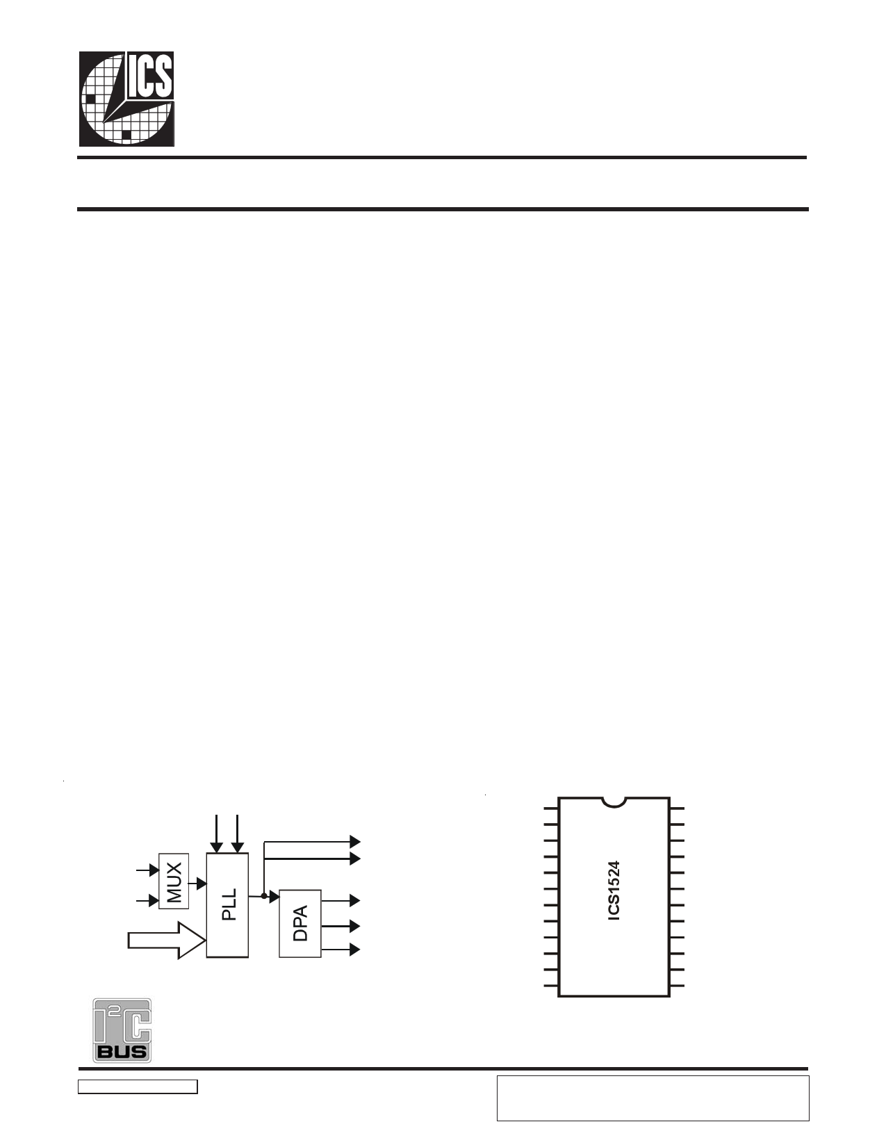
Block Diagram
Pin Configuration
HSYNC
OSC
I2C
Loop
Filter
CLK
CLK+/-
DPACLK
DPACLK+/-
FUNC
VDDD
VSSD
SDA
SCL
PDEN
EXTFB
HSYNC
EXTFIL
XFILRET
VDDA
VSSA
OSC
1
2
3
4
5
6
7
8
9
10
11
12
24 IREF
23 CLK+ (PECL)
22 CLK– (PECL)
21 DPACLK+ (PECL)
20 DPACLK– (PECL)
19 VSSQ
18 VDDQ
17 DPACLK (SSTL)
16 CLK
(SSTL)
15 FUNC (SSTL)
14 LOCK/REF (SSTL)
13 I2CADR
24 Pin 300-mil SOIC
I2C-bus is a trademark of Philips Corporation.
ICS1524 Rev C 01/31/2003
ICS reserves the right to make changes in the device data identified in this
publication without further notice. ICS advises its customers to obtain the
latest version of all device data to verify that any information being relied
upon by the customer is current and accurate.
1 page 
ICS1524
I2C Register Map Summary
Register
Index
0h
Name
Input Control
Access
R/W
Bit Name
PDen
PD_Pol
Ref_Pol
Fbk_Pol
Fbk_Sel
Func_Sel
E nP L S
E nD L S
Bit #
0
1
2
3
4
5
6
7
Reset
Value
Description
1 Phase Detector Enable
(0=Disable 1=Enable)
0 Phase Detector Input Select
0 External Reference Polarity (0=Positive Edge, 1=Negative Edge)
0 External Feedback Polarity (0=Positive Edge, 1=Negative Edge)
0 External Feedback Select
(0=Internal Feedback, 1=External)
0 Function Out Select
(0=Recovered HSYNC, 1=Input HSYNC)
1 Enable PLL Lock/Ref Status Output
(0=Disable 1=Enable)
0 Enable DPA Lock/Ref Status Output
(0=Disable 1=Enable)
1h
Loop Control R / W * PFD0-2
0-2
0 Phase Detector Gain
Reserved
3
0 Reserved
PSD0-1 4-5 0 Post-Scaler Divider
Reserved
6-7
0 Reserved
(0 = /2, 1 = /4, 2 = /8, 3 = /16)
2h FdBk Div 0
R / W * FBD0-7
0-7 FF PLL FeedBack Divider LSBs (bits 0-7) *
3h FdBk Div 1
R/W*
FBD8-11
Reserved
0-3
4-7
F PLL Feedback Divider MSBs (bits 8-11) *
0 Reserved
4h DPA Offset
R/W
DPA_OS0-5
Reserved
Fil_Sel
0-5
6
7
0 Dynamic Phase Aligner Offset
0 Reserved
1 Loop Filter Select
(0=External, 1=Internal)
5h DPA Control R / W ** DPA_Res0-1 0-1 3 DPA Resolution (0=16 delay elements, 1=32, 2=Reserved, 3=64)
Metal_Rev 2-7
0 Metal Mask Revision Number
6h
Output Enables R / W
OE_Pck
0
1 Output Enable for PECL DPACLK
( 0=High Z, 1=Enabled)
OE_Tck
1
1 Output Enable for STTL_3 DPACLK
( 0=High Z, 1=Enabled)
OE_P2 2 1 Output Enable for PECL CLK
( 0=High Z, 1=Enabled)
OE_T2 3 1 Output Enable for STTL_3 CLK
( 0=High Z, 1=Enabled)
OE_F
4 1 Output Enable for STTL_3 FUNC
( 0=High Z, 1=Enabled)
Ck2_Inv 5 0 Select non-delayed CLK (1) or DPA delayed CLK/2 (0) on CLKx pins
Out_Scl 6-7 0 SSTL DPACLK (Pin 17) Scaler (0 = ÷1, 1 = ÷2, 2 = ÷4, 3 = ÷8)
7h Osc_Div
R/W
Osc_Div 0-6
In-Sel
0-6
7
0 Osc Divider modulus
1 RESERVED
8h Reset
Write
DPA
PLL
0-3 x Writing xA hex resets DPA and loads working register 5
4-7 x Writing 5x hex resets PLL and loads working registers 1-3
10h Chip Ver
Read Chip Ver 0-7 18 Chip Version 17 hex
11h Chip Rev
Read Chip Rev 0-7 01 Chip Revision C2 hex
12h Rd_Reg
Read
DPA_Lock
PLL_Lock
Reserved
0
1
2-7
N/A DPA Lock Status
N/A PLL Lock Status
0 Reserved
(0=Unlocked, 1=Locked)
(0=Unlocked, 1=Locked)
* Identifies double-buffered registers. Working registers are loaded during software PLL reset.
** Identifies double-buffered register. Working registers are loaded during software DPA reset.
ICS1524 Rev C 01/31/2003
5
5 Page 
ICS1524
Name: Oscillator Divider Register
Register: 7h
Index: Read / Write
Bit Name
Osc_Div 0-6
In_Sel
Bit #
0-6
7
Reset Value
0
1
Description
Osc Divider Modulus
Input Select
Bit Name
Description
0 - 6 Osc_Div 0-6 Oscillator Divider Modulus.
Divides the input from OSC (pin 12) by the set modulus.
The modulus equals the programmed value, plus 2.
Therefore, the modulus range is from 3 to 129.
7 In_Sel
Input Select — Selects the input to the Phase/Frequency Detector
0 = HSYNC
1 = Osc Divider
Name: RESET Register
Register: 8 h
Index: Write
Bit Name
DPA Reset
PLL Reset
Bit #
0-3
4 -7
Reset Value
x
x
Description
Writing xAh to this register resets DPA working register 5
Writing 5xh to this register resets PLL working registers 1-3
Bit Name
0 - 3 DPA
4 -7 PLL
Description
Writing xAh to this register resets DPA working register 5
Writing 5xh to this register resets PLL working registers 1-3
Value
xA
5x
5A
Resets
DPA
PLL
DPA and PLL
ICS1524 Rev C 01/31/2003
11
11 Page | ||
| Páginas | Total 24 Páginas | |
| PDF Descargar | [ Datasheet ICS1524.PDF ] | |
Hoja de datos destacado
| Número de pieza | Descripción | Fabricantes |
| ICS1522 | User-Programmable Video Clock Generator/ Line-Locked Clock Regenerator | Integrated Circuit Systems |
| ICS1523 | High-Performance Programmable Line-Locked Clock Generator | Integrated Circuit Systems |
| ICS1524 | Dual Output Phase Controlled SSTL-3/PECL Clock Generator | Integrated Circuit Systems |
| ICS1526 | Video Clock Synthesizer | Integrated Circuit Systems |
| Número de pieza | Descripción | Fabricantes |
| SLA6805M | High Voltage 3 phase Motor Driver IC. |
Sanken |
| SDC1742 | 12- and 14-Bit Hybrid Synchro / Resolver-to-Digital Converters. |
Analog Devices |
|
DataSheet.es es una pagina web que funciona como un repositorio de manuales o hoja de datos de muchos de los productos más populares, |
| DataSheet.es | 2020 | Privacy Policy | Contacto | Buscar |