|
|
|
PDF ICS1531 Data sheet ( Hoja de datos )
| Número de pieza | ICS1531 | |
| Descripción | Triple 8-bit MSPS A/D Converters with Line-Locked Clock Generator | |
| Fabricantes | Integrated Circuit Systems | |
| Logotipo | ||
Hay una vista previa y un enlace de descarga de ICS1531 (archivo pdf) en la parte inferior de esta página. Total 30 Páginas | ||
|
No Preview Available !
Integrated Circuit Systems, Inc.
ICS1531 1531
Document Type: Data Sheet
Document Stage: Preliminary Product Preview
Triple 8-bit MSPS A/D Converters with Line-Locked Clock Generator
General Description
Features
The ICS1531 is a high-performance, cost-effective,
3-channel, 8-bit analog-to-digital converter with an
integrated line-locked clock generator. It is part of a family
of chips intended for high-resolution video applications that
use analog inputs, such as LCD monitors, LCD projectors,
plasma displays, and projection TVs. Using ICS's
low-voltage CMOS mixed-signal technology, the ICS1531
is an effective data-capture solution for resolutions from
VGA to UXGA.
The ICS1531 offers analog-to-digital data conversion and
synchronized pixel clock generation at speeds of 100, 140, or
165 MHz (or mega samples per second, MSPS). The
Dynamic Phase Adjust (DPA) circuitry allows end-user
control over the pixel clock phase, relative to the recovered
sync signal and analog pixel data. Either the internal pixel
clock can be used as a capture clock input to the
analog-to-digital converters or an external clock input can be
used. The ICS1531 provides either one or two 24-bit pixels
per clock. An ADCSYNC output pin provides recovered
HSYNC from the pixel clock phase-locked-loop (PLL)
divider chain output, which can be used to synchronize
display enable output.
A clamp signal can be generated internally or provided
through the CLAMP pin. A high-bandwidth video amplifier
with adjustable gain allows fine tuning of the analog signal.
The advanced PLL uses an internal programmable feedback
divider. Two additional, independent programmable PLLs,
each with spread-spectrum functionality, support memory
and panel clock requirements.
• 3-channel 8-bit analog-to-digital conversion up to 165 MHz
• Direct connection to analog input data (no external
pre-amplifier circuit needed)
• Video amplifier: 500-MHz analog bandwidth,
software-adjustable gain
• Dynamic Phase Adjust (DPA) for software-adjustable
analog sample points
• Software selectable: One pixel per clock (for 24-bit
pixels) or two pixels per clock (for a total of 48 bits)
• Internal clamp circuit. Very low jitter.
• Low-voltage TTL clock outputs, synchronized with
digital pixel data outputs
• Independent software reset for PLLs and DPA
• Double-buffered PLL and DPA control registers
• Two additional PLLs with spread spectrum for memory
and panel clock
• External/internal loop-filter selection with software
• Automatic Power-On Reset (POR) detection
• Uses 3.3 VDC. Digital inputs are 5-V tolerant.
• Industry-standard 2-wire serial bus interface speeds:
low (100 kHz), high (400 kHz), or ultra (800 kHz)
• Lock detection available in hardware and software
• 144-pin low-profile quad flat pack (LQFP) package
Applications
• LCD displays, LCD projectors, plasma displays, and
projection TVs
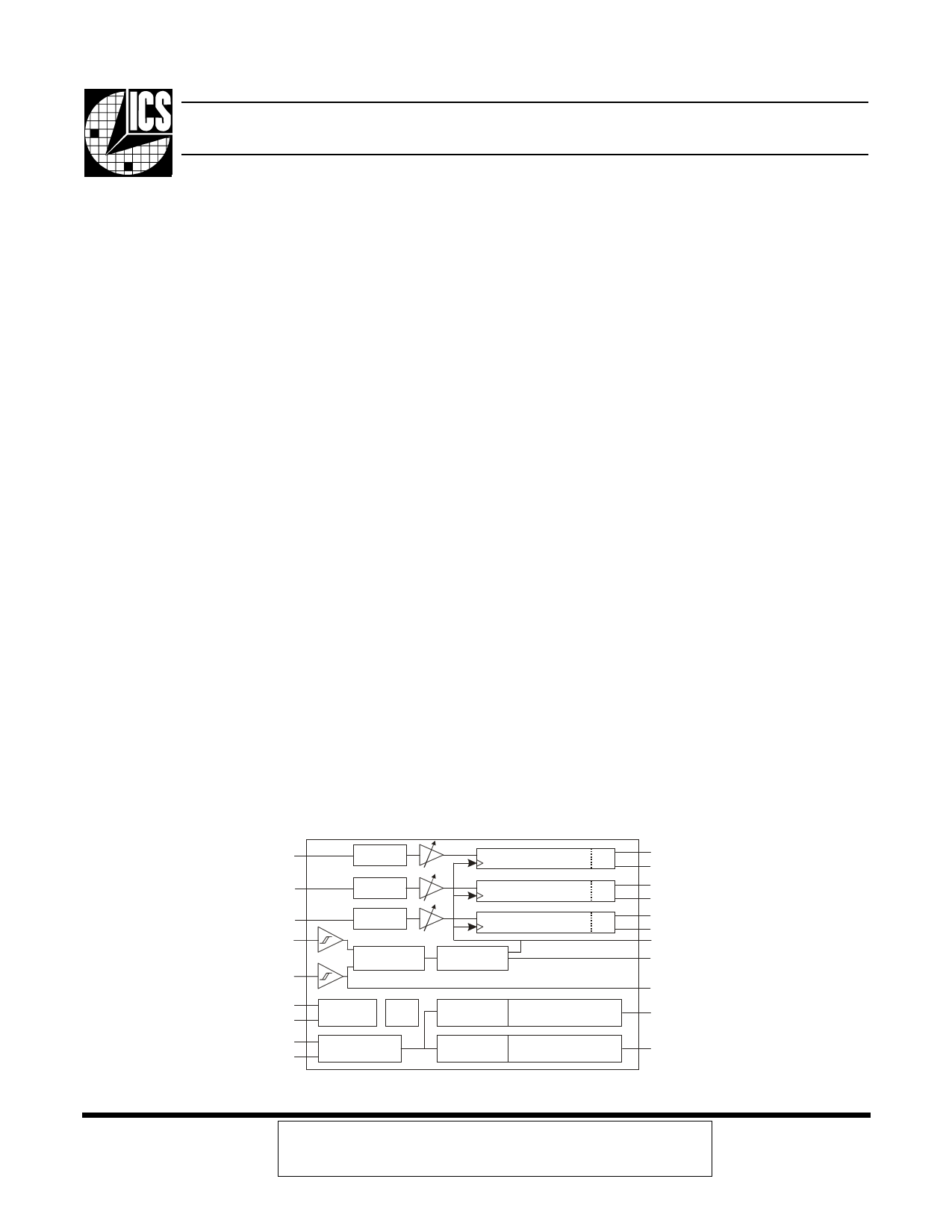
ICS1531
Functional
Block Diagram
Red
Green
Blue
VSYNC
HSYNC
SDA
SCL
XTAL In
XTAL O ut
CLAMP
CLAMP
CLAMP
PLL
Serial IF POR
Crystal
O s c illa t o r
ADC
ADC
ADC
D PA
PLL
PLL
Spread Spectrum
Spread Spectrum
RA0-RA7
RB0-RB7
G A 0 -G A 7
G B 0 -G B 7
B A 0 -B A 7
B B 0 -B B 7
AD C R C LK
ADCSYNC
REF
MCLK
PNLCLK
ICS1531 Rev N 12/1/99
December 8, 2000 2:31pm
PRODUCT PREVIEW documents contain information on new products in
the sampling or preproduction phase of development. Characteristic data
and other specifications are subject to change without notice.
December, 1999
1 page 
ICS1531 Data Sheet - Preliminary
Chapter 2 Summary
2.3 Phase-Locked Loop (Generates Pixel Clock from Input HSYNC)
The ICS1531 uses a phase-locked loop (PLL) to generate its pixel clock output frequency. A PLL is a
closed-loop feedback system that locks an output signal’s phase and frequency to that of a reference input
signal’s phase and frequency. In the case of the ICS1531, when its PLL is locked it locks a pixel clock
output to that of an HSYNC signal from input video.For a block diagram of the ICS1531 PLL, see Figure 4-1
and Figure 4-2.
2.3.1 Phase/Frequency Detector (Compares Two Input Signals)
The first section of the PLL is the Phase/Frequency Detector (PFD). To use the PLL, first the PFD must be
enabled either through hardware control (with a signal from the PDEN pin) or software control (Reg 00:1-0).
Once the PFD is enabled, the PFD compares both the phase and frequency of the following two input
signals.
• PFD Input Signal 1: External HSYNC Signal or Internal Oscillator Signal
The first input to the PFD can be selected from either the external HSYNC signal or the ICS1531 internal
crystal oscillator signal (Reg 00:5).
– External HSYNC signal
Typically, one of the input signals to the PFD comes from the HSYNC of a PC display controller. This
input HSYNC signal can have a transition time of tens of nanoseconds. Furthermore, if the input
HSYNC signal is from a remote source, its pulses can degrade.
A high-performance Schmitt trigger (Reg 00:7-6) conditions the HSYNC pulse before it is input to the
PFD. The polarity of this input pulse can be programmed (Reg 00:2). The result of this conditioning
is REF, a clean reference clock signal that in comparison to the input HSYNC signal has a short
transition time. [For more information on adjusting the HSYNC signal, see Section 2.6, “Dynamic
Phase Adjust (Positions Pixel Clock on Sub-Pixel Basis)”.]
– Internal crystal oscillator
Alternatively, one of the input signals to the PFD can be from the ICS1531 internal crystal oscillator
(Regs 07:7-0 and 2C:6-4).
• PFD Input Signal 2: Signal from Feedback Loop
The second input to the PFD comes from the output of the PLL feedback loop, which results from the
processing that takes place with the charge pump, filter, voltage-controlled oscillator, post-scaler divider,
and feedback divider. That is, the PLL output (the signal from the feedback loop) also appears as one of
the two inputs to the PFD.
As a result of the comparison of the two input signals, the PFD processes the inputs so there is the proper
ratio between them. Then the PFD uses the output to drive a charge pump.
2.3.2 Charge Pump (Boosts Voltage Gain of Signal from PFD)
The charge pump, which is a current-source and current-sink pair, boosts the voltage gain of the signal
from the PFD. This PFD signal gain is programmable over a 7-bit range up to 128 µA (Reg 01:2-0).
2.3.3 Loop Filter (Filters Output from Charge Pump)
The loop filter, which is a capacitance and resistance in series, acts as a low-bandpass filter for the
frequency output from the charge pump. The ICS1531 can select between either an external loop filter, or
more typically, an internal loop filter (Reg 08:0). The advantage of the internal filter is that it can be used for
all Video Electronics Standards Association (VESA) timing modes, for ease in manufacturing.
Note:
VESA establishes standard timing specifications for the personal-computer industry. Although
many computer manufacturers require that display controllers adhere to the VESA timing
specifications, there is no enforcement. As a result, not all display controllers conform precisely
to the VESA timing specifications.
ICS1531 Rev N 12/1/99
Copyright © 1999, Integrated Circuit Systems, Inc.
All rights reserved.
December, 1999
5
5 Page 
ICS1531 Data Sheet - Preliminary
Chapter 3 Pin Diagram and Listings
3.2.2 Pin Listing by Alphabetical Pin Name
Note:
1. The TRESET pin was formerly a Reserved pin.
2. The following pins, formerly ‘Reserved’, are now NC (No Connect): 4, 11, 18, 97–98, 117–133, 136
3. The (active-low) STATUS pin was formerly called ‘LOCK’.
Table 3-2. ICS1531 Pins, by Alphabetical Pin Name
Pin Name
ABLUE
Pin No.
22
Pin Name
GB3
Pin No.
60
ADCRCLK
54
GB4
59
ADCSYNC
55
GB5
58
AGRN
19
GB6
51
ARED
15
GB7
50
BA0 49 HSYNC
6
BA1 48 MCLK
101
BA2 47 NC
BA3 46
4, 11, 18, 97–98,
117–133, 136
BA4 43 OSCOUT
113
BA5 42 PDEN
141
BA6 41 PNLCLK
104
BA7 40 PSEL1
8
BB0 39 PSEL2
9
BB1 38 PSEL3
10
BB2 35 RA0
95
BB3 34 RA1
94
BB4 33 RA2
93
BB5 32 RA3
92
BB6 31 RA4
91
BB7 30 RA5
90
CLAMP
28
RA6
87
CLK 114 RA7
86
EXTFIL
144
RB0
85
GA0
75
RB1
84
GA1
74
RB2
83
GA2
71
RB3
82
GA3
70
RB4
79
GA4
69
RB5
78
GA5
68
RB6
77
GA6
67
RB7
76
GA7
66
REF
112
GB0
63
Reserved
14, 21, 115
GB1
62
SBADR
142
GB2
61
SCL
137
Pin Name
SDA
STATUS
TRESET
VDDA
VDDAADC
VDDD
VDDDADC
VDDMCLK
VDDPCLK
VDDQ
VDDQADC
VDDXTL
VRB
VRTB
VRTG
VRTR
VSS
VSSA
VSSAADC
VSSD
VSSDADC
VSSMCLK
VSSPCLK
VSSQ
VSSQADC
VSSSUB
VSS(TEST)
VSSXTL
XFILRET
XIN
XOUT
Pin No.
138
111
2
134
24, 27
140
53
100
103
109
29, 37, 45, 57,
65, 73, 81, 89
108
17
23
20
16
1, 3, 5
135
25, 26, 96
139
52
99
102
110
36, 44, 56, 64,
72, 80, 88
7, 13, 116
12
105
143
106
107
ICS1531 Rev N 12/1/99
Copyright © 1999, Integrated Circuit Systems, Inc.
All rights reserved.
December, 1999
11
11 Page | ||
| Páginas | Total 30 Páginas | |
| PDF Descargar | [ Datasheet ICS1531.PDF ] | |
Hoja de datos destacado
| Número de pieza | Descripción | Fabricantes |
| ICS1531 | Triple 8-bit MSPS A/D Converters with Line-Locked Clock Generator | Integrated Circuit Systems |
| Número de pieza | Descripción | Fabricantes |
| SLA6805M | High Voltage 3 phase Motor Driver IC. |
Sanken |
| SDC1742 | 12- and 14-Bit Hybrid Synchro / Resolver-to-Digital Converters. |
Analog Devices |
|
DataSheet.es es una pagina web que funciona como un repositorio de manuales o hoja de datos de muchos de los productos más populares, |
| DataSheet.es | 2020 | Privacy Policy | Contacto | Buscar |