|
|
|
PDF ICS950812 Data sheet ( Hoja de datos )
| Número de pieza | ICS950812 | |
| Descripción | Frequency Generator with 200MHz Differential CPU Clocks | |
| Fabricantes | Integrated Circuit Systems | |
| Logotipo | ||
Hay una vista previa y un enlace de descarga de ICS950812 (archivo pdf) en la parte inferior de esta página. Total 29 Páginas | ||
|
No Preview Available !
Integrated
Circuit
Systems, Inc.
ICS950812
Frequency Generator with 200MHz Differential CPU Clocks
Recommended Application:
Pin Configuration
CK-408 clock with Buffered/Unbuffered mode supporting
Almador, Brookdale, ODEM, and Montara-G chipsets with
PIII/P4 processor. Programmable for group to group skew.
Output Features:
• 3 Differential CPU Clock Pairs @ 3.3V
• 7 PCI (3.3V) @ 33.3MHz including 2 early PCI clocks
• 3 PCI_F (3.3V) @ 33.3MHz
• 1 USB (3.3V) @ 48MHz, 1 DOT (3.3V) @ 48MHz
• 1 REF (3.3V) @ 14.318MHz
• 5 3V66 (3.3V) @ 66.6MHz
• 1 VCH/3V66 (3.3V) @ 48MHz or 66.6MHz
• 3 66MHz_OUT/3V66 (3.3V) @ 66.6MHz_IN or 66.6MHz
Features:
• Provides standard frequencies and additional 5%
and 10% over-clocked frequencies
• Supports spread spectrum modulation:
No spread, Center Spread (±0.35%, ±0.5%,
or ±0.75%), or Down Spread (-0.5%, -1.0%, or -1.5%)
• Offers adjustable PCI early clock via latch inputs
• Selectable 1X or 2X strength for REF via I2C interface
• Efficient power management scheme through PD#,
CPU_STOP# and PCI_STOP#.
• Uses external 14.318MHz crystal
VDDREF 1
X1 2
X2 3
GND 4
PCICLK_F0 5
PCICLK_F1 6
PCICLK_F2 7
VDDPCI 8
GND 9
PCICLK0 10
**E_PCICLK1/PCICLK1 11
PCICLK2 12
**E_PCICLK3/PCICLK3 13
VDDPCI 14
GND 15
PCICLK4 16
PCICLK5 17
PCICLK6 18
VDD3V66 19
GND 20
66MHZ_OUT0/3V66_2 21
66MHZ_OUT1/3V66_3 22
66MHZ_OUT2/3V66_4 23
66MHZ_IN/3V66_5 24
*PD# 25
VDDA 26
GND 27
Vtt_PWRGD# 28
56 REF
55 FS1
54 FS0
53 CPU_STOP#*
52 CPUCLKT0
51 CPUCLKC0
50 VDDCPU
49 CPUCLKT1
48 CPUCLKC1
47 GND
46 VDDCPU
45 CPUCLKT2
44 CPUCLKC2
43 MULTSEL*
42 IREF
41 GND
40 FS2
39 48MHz_USB/FS3**
38 48MHz_DOT
37 VDD48
36 GND
35 3V66_1/VCH_CLK/FS4**
34 PCI_STOP#*
33 3V66_0/FS5**
32 VDD3V66
31 GND
30 SCLK
29 SDATA
• Stop clocks and functional control available through
I2C interface.
Key Specifications:
56-Pin 300mil SSOP
6.10 mm. Body, 0.50 mm. pitch TSSOP
• CPU Output Jitter <150ps
• 3V66 Output Jitter <250ps
*These inputs have 120K internal pull-up resistors to VDD.
**Internal pull-down resistors to ground.
• 66MHz Output Jitter (Additive) (Buffered Mode) <100ps
• CPU Output Skew <100ps
Note:
Almador board level designs MUST use pin 22,
66MHZ_OUT1, as the feedback connection from the
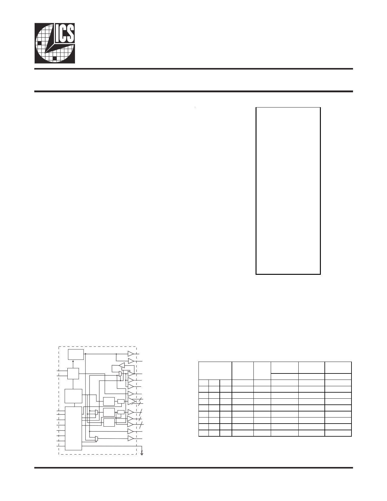
Block Diagram
clock buffer path to the Almador (GMCH) chipset.
PLL2
X1 XTAL
X2 OSC
PD#
CPU_STOP#
PCI_STOP#
MULTSEL
FS (5:0)
SDATA
SCLK
VTT_PWRGD#
PLL1
Spread
Spectrum
Control
Logic
Config.
Reg.
CPU
DIVDER
Stop
PCI
DIVDER
Stop
3V66
DIVDER
48MHz_USB
48MHz_DOT
3V66_5/66MHz_IN
3V66_3/66MHz_OUT1
3V66_(4,2)/66MHz_OUT(2,0)
REF
3 CPUCLKT (2:0)
3 CPUCLKC (2:0)
PCICLK (6:4, 2, 0)
7
E_PCICLK(1,3)/PCICLK(1,3)
2
3 PCICLK_F (2:0)
3V66_0
3V66_1/VCH_CLK
I REF
Frequency Select
Bit CPUCLK
FS2 FS1 FS0
00 0
00 1
01 0
01 1
10 0
10 1
11 0
11 1
MHz
66.66
100.00
200.00
133.33
66.66
100.00
200.00
133.33
3V66
MHz
66.66
66.66
66.66
66.66
66.66
66.66
66.66
66.66
66MHz_OU
T (2:0)
3V66 (4:2)
MHz
66.66
66.66
66.66
66.66
66MHz_IN
66MHz_IN
66MHz_IN
66MHz_IN
66MHz_IN PCICLK_F
3V66_5
MHz
66.66
66.66
66.66
66.66
Input
Input
Input
Input
PCICLK
MHz
33.33
33.33
33.33
33.33
66MHz_IN/2
66MHz_IN/2
66MHz_IN/2
66MHz_IN/2
0542G—08/21/03
1 page 
Maximum Allowed Current
Max 3.3V supply consumption
Condition
Max discrete cap loads,
Vdd = 3.465V
All static inputs = Vdd or GND
Powerdown Mode
(PD# = 0)
40mA
Active Full
280mA
Host Swing Select Functions
MULTSEL
Board Target
Trace/Term Z
Reference R,
Iref = VDD/3*Rr
Rr = 221 1%,
0
50 ohms
Iref = 5.00mA
1
50 ohms
Rr = 475 1%,
Iref = 2.32mA
Output
Current
Voh @ Z
Ioh = 4 * I REF
Ioh = 6 * I REF
1.0V @ 50 ohm
0.7V @ 50 ohm
PCI Select Functions
E_PCICLK1 (11) E_PCICLK3 (13)
00
01
10
11
Note:
E_PCICLK1 = 10Kohm resistor.
E_PCICLK3 = 10Kohm resistor.
0 = No resistor
1 = 10Kohm pull-up to VDD.
* Approximate values
E_PCICLK(3,1)*
0ns
0.5ns
1.0ns
1.5ns
ICS950812
0542G—08/21/03
5
5 Page 
ICS950812
Table 7
3V66 (0:1) I2C Control Table
CPU_STOP#
(Pin 53)
0
0
1
1
Byte 5
Bit 4
0
1
0
1
3V66 (1:0)
Running
Stopped
Running
Running
Note: Activating Byte 5, Bit 4 will allow CPU_STOP# to control stop of pins 33 and 35.
Table 8: Byte 11-14 Defaults
ADDRESS
FS5 FS4 FS3 FS1 FS0
00 0 0 0 0
10 0 0 0 1
20 0 0 1 0
30 0 0 1 1
40 0 1 0 0
50 0 1 0 1
60 0 1 1 0
70 0 1 1 1
80 1 0 0 0
90 1 0 0 1
10 0 1 0 1 0
11 0 1 0 1 1
12 0 1 1 0 0
13 0 1 1 0 1
14 0 1 1 1 0
15 0 1 1 1 1
16 1 0 0 0 0
17 1 0 0 0 1
18 1 0 0 1 0
19 1 0 0 1 1
20 1 0 1 0 0
21 1 0 1 0 1
22 1 0 1 1 0
23 1 0 1 1 1
24 1 1 0 0 0
25 1 1 0 0 1
26 1 1 0 1 0
27 1 1 0 1 1
28 1 1 1 0 0
29 1 1 1 0 1
30 1 1 1 1 0
31 1 1 1 1 1
CPU
Freq
66.66
99.99
199.98
133.32
66.50
99.75
199.50
133.00
66.34
99.51
199.02
132.68
66.16
99.23
198.47
132.31
66.66
99.99
199.98
133.32
66.66
99.99
199.98
133.32
70.00
105.00
210.00
140.00
73.33
109.99
219.98
146.65
Spread
Center
Down
Center
Center
Center
Center
Down
Down
Down
Down
Down
Down
Down
Down
Down
Down
Down
Down
Center
Center
Center
Center
Center
Center
Center
Center
Center
Center
Center
Center
Center
Center
Center
Center
0.40%
0.40%
0.40%
0.40%
-0.48%
-0.48%
-0.48%
-0.48%
-0.98%
-0.98%
-0.98%
-0.98%
-1.52%
-1.52%
-1.52%
-1.52%
0.51%
0.51%
0.51%
0.51%
0.74%
0.74%
0.74%
0.74%
0.35%
0.35%
0.35%
0.35%
0.34%
0.34%
0.34%
0.34%
I2C read back values in Hex.
Bytes
I2C read back values in binary.
11 12 13 14 11 12 13 14
8D 9B 02 18 10001101 10011011 00000010 00011000
8D 9B 02 18 10001101 10011011 00000010 00011000
8D 9B 02 18 10001101 10011011 00000010 00011000
8D 9B 02 18 10001101 10011011 00000010 00011000
8D 9A EF 17 10001101 10011010 11101111 00010111
8D 9A EF 17 10001101 10011010 11101111 00010111
8D 9A EF 17 10001101 10011010 11101111 00010111
8D 9A EF 17 10001101 10011010 11101111 00010111
8D 99 E7 17 10001101 10011001 11100111 00010111
8D 99 E7 17 10001101 10011001 11100111 00010111
8D 99 E7 17 10001101 10011001 11100111 00010111
8D 99 E7 17 10001101 10011001 11100111 00010111
90 EB DD 17 10010000 11101011 11011101 00010111
90 EB DD 17 10010000 11101011 11011101 00010111
90 EB DD 17 10010000 11101011 11011101 00010111
90 EB DD 17 10010000 11101011 11011101 00010111
8D 9B 05 18 10001101 10011011 00000101 00011000
8D 9B 05 18 10001101 10011011 00000101 00011000
8D 9B 05 18 10001101 10011011 00000101 00011000
8D 9B 05 18 10001101 10011011 00000101 00011000
8D 9B 0B 18 10001101 10011011 00001011 00011000
8D 9B 0B 18 10001101 10011011 00001011 00011000
8D 9B 0B 18 10001101 10011011 00001011 00011000
8D 9B 0B 18 10001101 10011011 00001011 00011000
8D B0 35 19 10001101 10110000 00110101 00011001
8D B0 35 19 10001101 10110000 00110101 00011001
8D B0 35 19 10001101 10110000 00110101 00011001
8D B0 35 19 10001101 10110000 00110101 00011001
89 4A 68 1A 10001001 01001010 01101000 00011010
89 4A 68 1A 10001001 01001010 01101000 00011010
89 4A 68 1A 10001001 01001010 01101000 00011010
89 4A 68 1A 10001001 01001010 01101000 00011010
0542G—08/21/03
11
11 Page | ||
| Páginas | Total 29 Páginas | |
| PDF Descargar | [ Datasheet ICS950812.PDF ] | |
Hoja de datos destacado
| Número de pieza | Descripción | Fabricantes |
| ICS950810 | Frequency Generator with 200MHz Differential CPU Clocks | Integrated Circuit Systems |
| ICS950812 | Frequency Generator with 200MHz Differential CPU Clocks | Integrated Circuit Systems |
| Número de pieza | Descripción | Fabricantes |
| SLA6805M | High Voltage 3 phase Motor Driver IC. |
Sanken |
| SDC1742 | 12- and 14-Bit Hybrid Synchro / Resolver-to-Digital Converters. |
Analog Devices |
|
DataSheet.es es una pagina web que funciona como un repositorio de manuales o hoja de datos de muchos de los productos más populares, |
| DataSheet.es | 2020 | Privacy Policy | Contacto | Buscar |