|
|
|
PDF IRLML5203 Data sheet ( Hoja de datos )
| Número de pieza | IRLML5203 | |
| Descripción | HEXFET Power MOSFET | |
| Fabricantes | International Rectifier | |
| Logotipo | ||
Hay una vista previa y un enlace de descarga de IRLML5203 (archivo pdf) en la parte inferior de esta página. Total 9 Páginas | ||
|
No Preview Available !
PROVISIONAL
l Ultra Low On-Resistance
l P-Channel MOSFET
l Surface Mount
l Available in Tape & Reel
l Low Gate Charge
Description
These P-channel MOSFETs from International Rectifier
utilize advanced processing techniques to achieve the
extremely low on-resistance per silicon area. This
benefit provides the designer with an extremely efficient
device for use in battery and load management
applications.
A thermally enhanced large pad leadframe has been
incorporated into the standard SOT-23 package to
produce a HEXFET Power MOSFET with the industry's
smallest footprint. This package, dubbed the Micro3TM,
is ideal for applications where printed circuit board
space is at a premium. The low profile (<1.1mm) of
the Micro3 allows it to fit easily into extremely thin
application environments such as portable electronics
and PCMCIA cards. The thermal resistance and
power dissipation are the best available.
VDSS
-30V
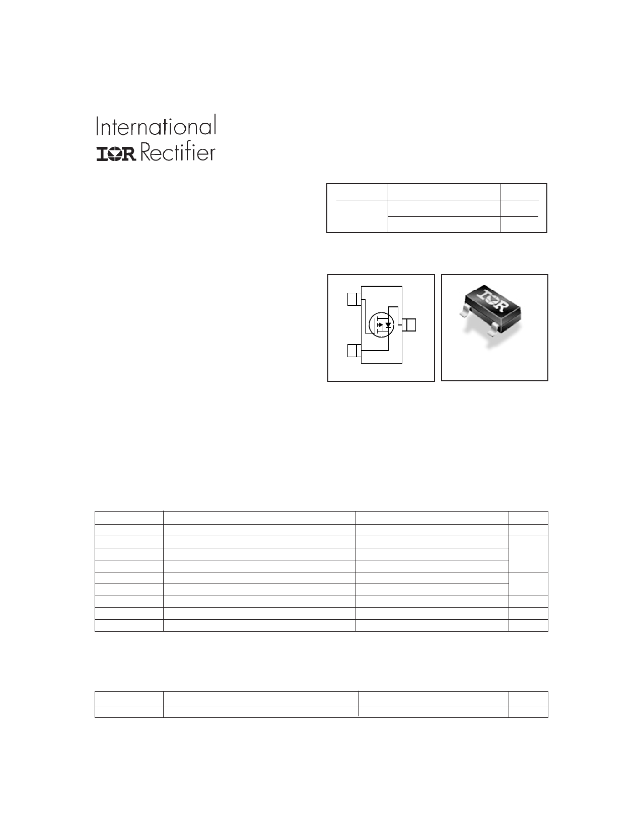
G1
S2
PD - 93967
IRLML5203
HEXFET® Power MOSFET
RDS(on) max (mΩ)
98@VGS = -10V
165@VGS = -4.5V
ID
-3.0A
-2.6A
3D
Micro3TM
Absolute Maximum Ratings
VDS
ID @ TA = 25°C
ID @ TA= 70°C
IDM
PD @TA = 25°C
PD @TA = 70°C
VGS
TJ, TSTG
Parameter
Drain- Source Voltage
Continuous Drain Current, VGS @ -10V
Continuous Drain Current, VGS @ -10V
Pulsed Drain Current
Power Dissipation
Power Dissipation
Linear Derating Factor
Gate-to-Source Voltage
Junction and Storage Temperature Range
Max.
-30
-3.0
-2.4
-24
1.25
0.80
10
± 20
-55 to + 150
Units
V
A
W
mW/°C
V
°C
Thermal Resistance
RθJA
www.irf.com
Parameter
Maximum Junction-to-Ambient
Max.
100
Units
°C/W
1
8/28/00
1 page 
PROVISIONAL
IRLML5203
3.0
2.0
1.0
0.0
25
50 75 100 125
TC , Case Temperature ( °C)
150
Fig 9. Maximum Drain Current Vs.
Case Temperature
1000
VDS
VGS
RG
RD
D.U.T.
VGS
Pulse Width ≤ 1 µs
Duty Factor ≤ 0.1 %
-
+ VDD
Fig 10a. Switching Time Test Circuit
VGS
10%
td(on) tr
td(off) tf
90%
VDS
Fig 10b. Switching Time Waveforms
100
D = 0.50
0.20
10 0.10
0.05
0.02
0.01
1
0.1
0.00001
PDM
t1
SINGLE PULSE
(THERMAL RESPONSE)
Notes:
1. Duty factor D = t1 / t 2
2. Peak T J = P DM x Z thJA + TA
t2
0.0001
0.001
0.01
0.1
t1, Rectangular Pulse Duration (sec)
1
Fig 11. Maximum Effective Transient Thermal Impedance, Junction-to-Ambient
www.irf.com
10
5
5 Page | ||
| Páginas | Total 9 Páginas | |
| PDF Descargar | [ Datasheet IRLML5203.PDF ] | |
Hoja de datos destacado
| Número de pieza | Descripción | Fabricantes |
| IRLML5203 | HEXFET Power MOSFET | International Rectifier |
| IRLML5203GPbF | Power MOSFET ( Transistor ) | International Rectifier |
| IRLML5203PBF | Power MOSFET ( Transistor ) | International Rectifier |
| Número de pieza | Descripción | Fabricantes |
| SLA6805M | High Voltage 3 phase Motor Driver IC. |
Sanken |
| SDC1742 | 12- and 14-Bit Hybrid Synchro / Resolver-to-Digital Converters. |
Analog Devices |
|
DataSheet.es es una pagina web que funciona como un repositorio de manuales o hoja de datos de muchos de los productos más populares, |
| DataSheet.es | 2020 | Privacy Policy | Contacto | Buscar |