|
|
|
PDF ICS9248-81 Data sheet ( Hoja de datos )
| Número de pieza | ICS9248-81 | |
| Descripción | Frequency Generator & Integrated Buffers | |
| Fabricantes | Integrated Circuit Systems | |
| Logotipo | ||
Hay una vista previa y un enlace de descarga de ICS9248-81 (archivo pdf) en la parte inferior de esta página. Total 18 Páginas | ||
|
No Preview Available !
Integrated
Circuit
Systems, Inc.
ICS9248- 81
Frequency Generator & Integrated Buffers
General Description
The ICS9248-81 is the single chip clock solution for Desktop/
Notebook designs using the SIS style chipset. It provides all
necessary clock signals for such a system.
Spread spectrum may be enabled through I2C programming.
Spread spectrum typically reduces system EMI by 8dB to
10dB. This simplifies EMI qualification without resorting to
board design iterations or costly shielding. The ICS9248-81
employs a proprietary closed loop design, which tightly
controls the percentage of spreading over process and
temperature variations.
Serial programming I2C interface allows changing functions,
stop clock programming and frequency selection. The SD_SEL
latched input allows the SDRAM frequency to follow the
CPUCLK frequency(SD_SEL=1) or other clock frequencies
(SD_SEL=0)
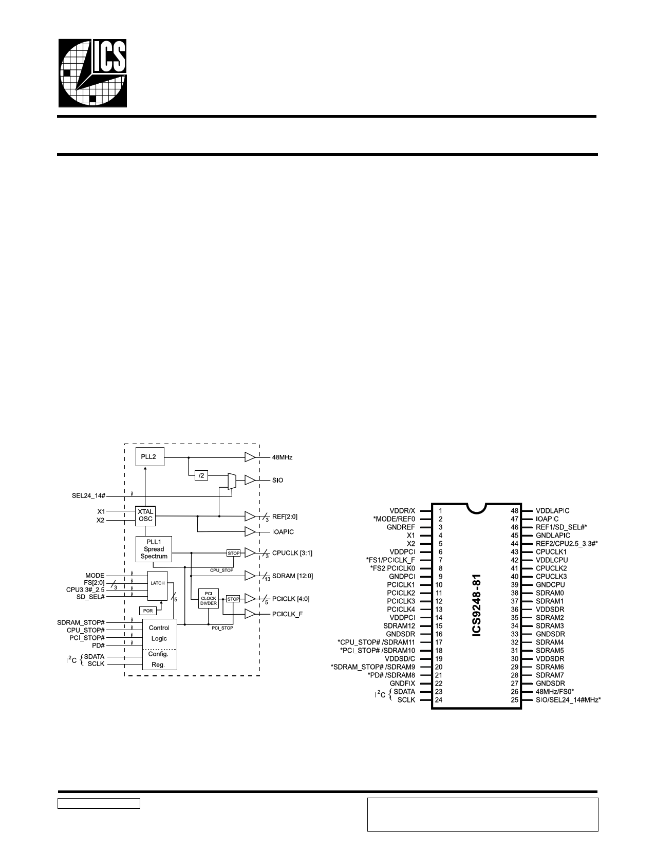
Block Diagram
Features
Generates the following system clocks:
- 3 CPU(2.5V/3.3V) up to 133.3MHz.
- 6 PCI(3.3V) (including 1 free-running)
- 13 SDRAMs(3.3V) up to 133.3MHz.
- 3 REF (3.3V) @ 14.318MHz
- 1 clock @ 24/14.3 MHz selectable output for SIO
- 1 Fixed clock at 48MHz (3.3V)
- 1 IOAPIC @ 2.5V / 3.3V
Skew characteristics:
- CPU CPU<175ps
- SDRAM SDRAM < 250ps
- CPUSDRAM < 500ps
- CPU(early) PCI : 1-4ns (typ. 3ns)
- PCI PCI <500ps
Supports Spread Spectrum modulation ±0.25 & ±0.5%
center spread
Serial I2C interface for Power Management, Frequency
Select, Spread Spectrum.
Efficient Power management scheme through PCI,
SDRAM, CPU STOP CLOCKS and PD#.
Uses external 14.318MHz crystal
48 pin 300mil SSOP.
Pin Configuration
Power Groups
VDDREF = REF [2:0], X1, X2
VDDPCI = PCICLK_F, PCICLK [4:0]
VDDSD/C = SDRAM [11:0], supply for PLL core, 24 MHz, 48MHz
VDD/CPU = CPUCLK [3:1]
VDDLAPIC = IOAPIC
GNDFIX = Ground for fixed clock PLL and output buffers
9248-81 Rev E 10/12/99
48-Pin SSOP
* Internal Pull-up Resistor of
120K to 3.3V on indicated inputs
Pentium is a trademark of Intel Corporation
I2C is a trademark of Philips Corporation
ICS reserves the right to make changes in the device data identified in
this publication without further notice. ICS advises its customers to
obtain the latest version of all device data to verify that any
information being relied upon by the customer is current and accurate.
1 page 
ICS9248 - 81
General I2C serial interface information
The information in this section assumes familiarity with I2C programming.
For more information, contact ICS for an I2C programming application note.
How to Write:
Controller (host) sends a start bit.
Controller (host) sends the write address D2 (H)
ICS clock will acknowledge
Controller (host) sends a dummy command code
ICS clock will acknowledge
Controller (host) sends a dummy byte count
ICS clock will acknowledge
Controller (host) starts sending first byte (Byte 0)
through byte 5
ICS clock will acknowledge each byte one at a time.
Controller (host) sends a Stop bit
How to Read:
Controller (host) will send start bit.
Controller (host) sends the read address D3 (H)
ICS clock will acknowledge
ICS clock will send the byte count
Controller (host) acknowledges
ICS clock sends first byte (Byte 0) through byte 5
Controller (host) will need to acknowledge each byte
Controller (host) will send a stop bit
How to Write:
Controller (Host)
Start Bit
Address
D2(H)
Dummy Command Code
Dummy Byte Count
Byte 0
Byte 1
Byte 2
Byte 3
Byte 4
Byte 5
Stop Bit
ICS (Slave/Receiver)
ACK
ACK
ACK
ACK
ACK
ACK
ACK
ACK
ACK
How to Read:
Controller (Host)
Start Bit
Address
D3(H)
ACK
ACK
ACK
ACK
ACK
ACK
ACK
Stop Bit
ICS (Slave/Receiver)
ACK
Byte Count
Byte 0
Byte 1
Byte 2
Byte 3
Byte 4
Byte 5
Notes:
1. The ICS clock generator is a slave/receiver, I2C component. It can read back the data stored in the latches for verification.
Read-Back will support Intel PIIX4 "Block-Read" protocol.
2. The data transfer rate supported by this clock generator is 100K bits/sec or less (standard mode)
3. The input is operating at 3.3V logic levels.
4. The data byte format is 8 bit bytes.
5. To simplify the clock generator I2C interface, the protocol is set to use only "Block-Writes" from the controller. The
bytes must be accessed in sequential order from lowest to highest byte with the ability to stop after any complete byte
has been transferred. The Command code and Byte count shown above must be sent, but the data is ignored for those
two bytes. The data is loaded until a Stop sequence is issued.
6. At power-on, all registers are set to a default condition, as shown.
5
5 Page 
ICS9248 - 81
Shared Pin Operation -
Input/Output Pins
The I/O pins designated by (input/output) on the ICS9248-
81 serve as dual signal functions to the device. During initial
power-up, they act as input pins. The logic level (voltage)
that is present on these pins at this time is read and stored
into a 4-bit internal data latch. At the end of Power-On reset,
(seeAC characteristics for timing values), the device changes
the mode of operations for these pins to an output function.
In this mode the pins produce the specified buffered clocks
to external loads.
header may be used.
These figures illustrate the optimal PCB physical layout
options. These configuration resistors are of such a large
ohmic value that they do not effect the low impedance clock
signals. The layouts have been optimized to provide as little
impedance transition to the clock signal as possible, as it
passes through the programming resistor pad(s).
To program (load) the internal configuration register for
these pins, a resistor is connected to either the VDD (logic 1)
power supply or the GND (logic 0) voltage potential. A 10
Kilohm(10K) resistor is used to provide both the solid CMOS
programming voltage needed during the power-up
programming period and to provide an insignificant load on
the output clock during the subsequent operating period.
Figs. 1 and 2 show the recommended means of implementing
this function. In Fig. 1 either one of the resistors is loaded
onto the board (selective stuffing) to configure the devices
internal logic. Figs. 2a and b provide a single resistor loading
option where either solder spot tabs or a physical jumper
Fig. 1
11
11 Page | ||
| Páginas | Total 18 Páginas | |
| PDF Descargar | [ Datasheet ICS9248-81.PDF ] | |
Hoja de datos destacado
| Número de pieza | Descripción | Fabricantes |
| ICS9248-80 | Frequency Generator & Integrated Buffers | Integrated Circuit Systems |
| ICS9248-81 | Frequency Generator & Integrated Buffers | Integrated Circuit Systems |
| ICS9248-87 | Frequency Generator & Integrated Buffers | Integrated Circuit Systems |
| Número de pieza | Descripción | Fabricantes |
| SLA6805M | High Voltage 3 phase Motor Driver IC. |
Sanken |
| SDC1742 | 12- and 14-Bit Hybrid Synchro / Resolver-to-Digital Converters. |
Analog Devices |
|
DataSheet.es es una pagina web que funciona como un repositorio de manuales o hoja de datos de muchos de los productos más populares, |
| DataSheet.es | 2020 | Privacy Policy | Contacto | Buscar |