|
|
|
PDF ICS9248-153 Data sheet ( Hoja de datos )
| Número de pieza | ICS9248-153 | |
| Descripción | Frequency Generator & Integrated Buffers | |
| Fabricantes | Integrated Circuit Systems | |
| Logotipo | ||
Hay una vista previa y un enlace de descarga de ICS9248-153 (archivo pdf) en la parte inferior de esta página. Total 14 Páginas | ||
|
No Preview Available !
Integrated
Circuit
Systems, Inc.
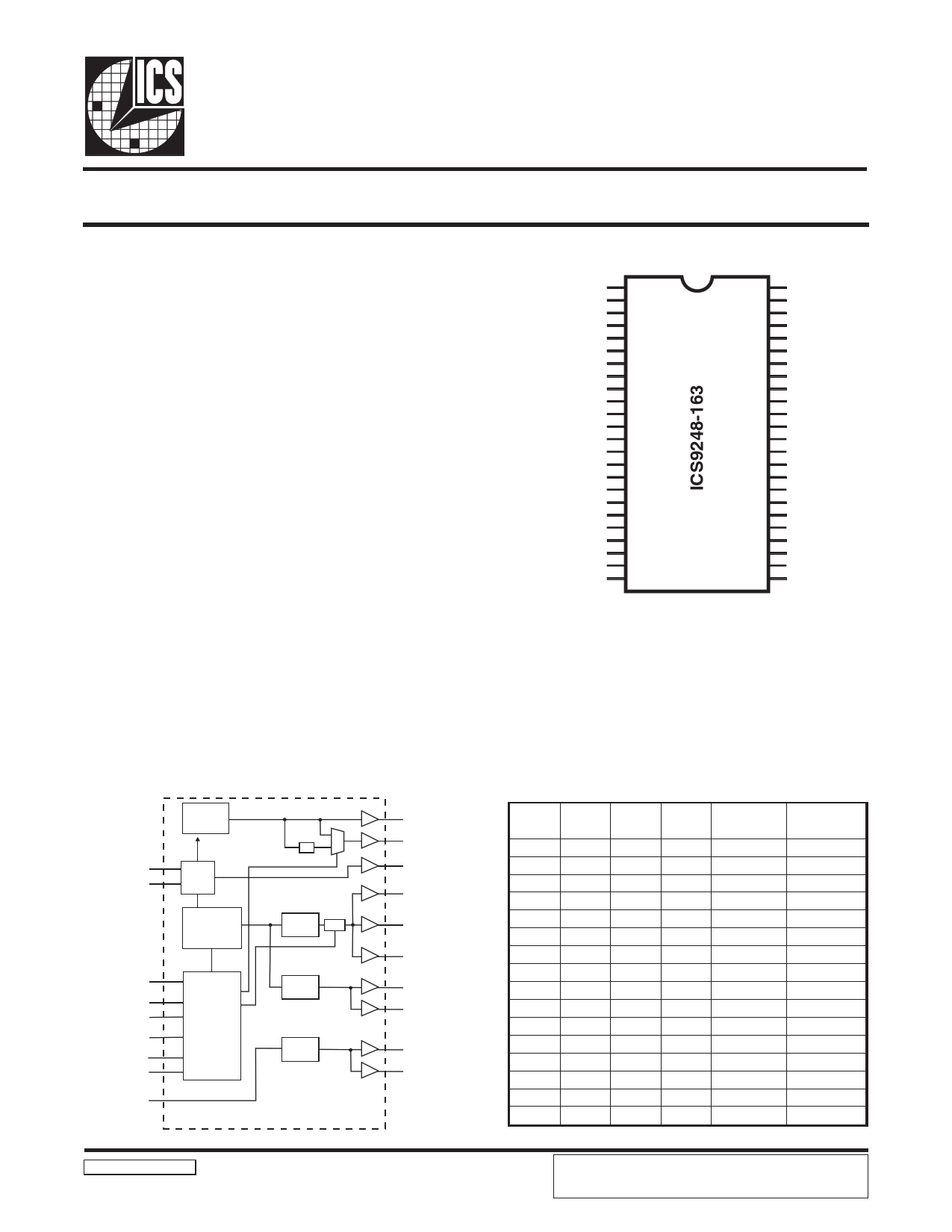
ICS9248-163
Preliminary Product Preview
AMD - K7 System Clock Chip
Recommended Application:
VIA KX133 style chipset
Output Features:
• 1 - Differential pair open drain CPU clocks
• 1 - CPU clock @ 3.3V
• 13 - SDRAM @ 3.3V
• 6 - PCI @3.3V,
• 1 - 48MHz, @3.3V fixed.
• 1 - 24/48MHz @ 3.3V
• 2 - REF @3.3V, 14.318MHz.
Features:
• Up to 166MHz frequency support
• Support power management: CPU stop and Power down
Mode from I2C programming.
• Spread spectrum for EMI control
(± 0.25% center spread).
• Uses external 14.318MHz crystal
Pin Configuration
VDDREF
REF0/CPU_STOP*
GND
X1
X2
VDD
*MODE/PCICLK_F
*FS3/PCICLK0
GND
*SEL24_48#/PCICLK1
PCICLK2
PCICLK3
PCICLK4
VDDPCI
BUFFER IN
GND
SDRAM11
SDRAM10
VDDSDR
SDRAM9
SDRAM8
GND
SDATA
SCLK
1
2
3
4
5
6
7
8
9
10
11
12
13
14
15
16
17
18
19
20
21
22
23
24
48 REF1/FS2*
47 GND
46 CPUCLK
45 GND
44 CPUCLKC0
43 CPUCLKT0
42 VDDA
41 PD#*
40 SDRAM_OUT
39 GND
38 SDRAM0
37 SDRAM1
36 VDDSDR
35 SDRAM2
34 SDRAM3
33 GND
32 SDRAM4
31 SDRAM5
30 VDDSDR
29 SDRAM6
28 SDRAM7
27 VDD48
26 48MHz/FS0*
25 24/48MHz/FS1*
48-Pin 300mil SSOP
* Internal Pull-up Resistor of 120K to VDD
Block Diagram
PLL2
X1
X2
SEL24_48#
SDATA
SCLK
FS (3:0)
PD#
CPU_STOP#
BUFFER IN
XTAL
OSC
PLL1
Spread
Spectrum
Control
Logic
Config.
Reg.
/2
CPU
DIVDER
Stop
PCI
DIVDER
SDRAM
DRIVER
Functionality
48MHz
24_48MHz
REF (1:0)
CPUCLK
CPUCLKC0
CPUCLKT0
PCICLK (4:0)
PCICLK_F
SDRAM (11:0)
SDRAM_OUT
FS3 FS2 FS1 FS0
0000
000 1
00 10
00 11
0 100
0 10 1
0 110
0 111
10 0 0
100 1
10
10
10 11
1 10 0
110 1
1 1 10
1111
CPU
(MHz)
90.00
95.00
101.00
102.00
100.90
103.00
105.00
100.00
107.00
109.00
110.00
111.00
113.00
115.00
117.00
133.30
PCICLK
(MHz)
30.00
31.67
33.67
34.00
33.57
34.33
35.00
33.33
35.67
36.33
36.67
37.00
37.67
38.33
39.00
33.33
9248-163 Rev A 9/22/00
Third party brands and names are the property of their respective owners.
PRODUCT PREVIEW documents contain information on new
products in the sampling or preproduction phase of development.
Characteristic data and other specifications are subject to change
without notice.
1 page 
ICS9248-163
Preliminary Product Preview
Byte 1: CPU, Active/Inactive Register
(1= enable, 0 = disable)
BIT
Bit 7
Bit 6
Bit 5
Bit 4
Bit 3
Bit 2
Bit 1
Bit 0
PIN#
-
-
-
-
40
-
43,44
46
PWD
DESCRIPTION
X FS2#
1 (Reserved)
1 (Reserved)
X FS3#
1 SDRAM_OUT
X (SEL24_48#)#
CPUCLK0 enable (both
1 differential pair. "True" and
Complimentary")
1 CPUCLKT enable
Byte 2: PCI, Active/Inactive Register
(1= enable, 0 = disable)
BIT
Bit 7
Bit 6
Bit 5
Bit 4
Bit 3
Bit 2
Bit 1
Bit 0
PIN#
-
7
-
13
12
11
10
8
PWD
DESCRIPTION
X FS0#
1 PCICLK_F
1 (Reserved)
1 PCICLK4
1 PCICLK3
1 PCICLK2
1 PCICLK1
1 PCICLK0
Byte 3: SDRAM, Active/Inactive Register
(1= enable, 0 = disable)
BIT
Bit 7
Bit 6
Bit 5
Bit 4
Bit 3
Bit 2
Bit 1
Bit 0
PIN#
-
-
26
25
17
18
20
21
PWD
DESCRIPTION
1 (Reserved)
1 (Reserved)
1 48MHz
1 24_48MHz
1 SDRAM 11
1 SDRAM 10
1 SDRAM 9
1 SDRAM 8
Byte 4: SDRAM , Active/Inactive Register
(1= enable, 0 = disable)
BIT
Bit 7
Bit 6
Bit 5
Bit 4
Bit 3
Bit 2
Bit 1
Bit 0
PIN#
28
29
31
32
34
35
37
38
PWD
DESCRIPTION
1 SDRAM 7
1 SDRAM 6
1 SDRAM 5
1 SDRAM 4
1 SDRAM 3
1 SDRAM 2
1 SDRAM 1
1 SDRAM 0
Byte 5: Peripheral , Active/Inactive Register
(1= enable, 0 = disable)
BIT
Bit 7
Bit 6
Bit 5
Bit 4
Bit 3
Bit 2
Bit 1
Bit 0
PIN# PWD
DESCRIPTION
- 1 (Reserved)
- 1 (Reserved)
- 1 (Reserved)
- X MODE#
- X FS1#
- 1 (Reserved)
48 1 REF1
2 1 REF0
Notes:
1. Inactive means outputs are held LOW and are disabled
from switching.
2. Latched Frequency Selects (FS#) will be inverted logic
load of the input frequency select pin conditions.
Byte 6: Peripheral , Active/Inactive Register
(1= enable, 0 = disable)
BIT PIN# PWD
DESCRIPTION
Bit7 -
0 Reserved (Note)
Bit6 -
0 Reserved (Note)
Bit5 -
0 Reserved (Note)
Bit4 -
0 Reserved (Note)
Bit3 -
0 Reserved (Note)
Bit2 -
1 Reserved (Note)
Bit1 -
1 Reserved (Note)
Bit0 -
0 Reserved (Note)
Note: Dont write into this register, writing into this
register can cause malfunction
Third party brands and names are the property of their respective owners.
5
5 Page 
ICS9248-163
Preliminary Product Preview
Shared Pin Operation -
Input/Output Pins
The I/O pins designated by (input/output) on the ICS9248-
163 serve as dual signal functions to the device. During initial
power-up, they act as input pins. The logic level (voltage)
that is present on these pins at this time is read and stored
into a 5-bit internal data latch. At the end of Power-On reset,
(see AC characteristics for timing values), the device changes
the mode of operations for these pins to an output function.
In this mode the pins produce the specified buffered clocks
to external loads.
To program (load) the internal configuration register for these
pins, a resistor is connected to either the VDD (logic 1) power
supply or the GND (logic 0) voltage potential. A 10 Kilohm
(10K) resistor is used to provide both the solid CMOS
programming voltage needed during the power-up
programming period and to provide an insignificant load on
the output clock during the subsequent operating period.
Figure 1 shows a means of implementing this function when
a switch or 2 pin header is used. With no jumper is installed
the pin will be pulled high. With the jumper in place the pin
will be pulled low. If programmability is not necessary, than
only a single resistor is necessary. The programming resistors
should be located close to the series termination resistor to
minimize the current loop area. It is more important to locate
the series termination resistor close to the driver than the
programming resistor.
Programming
Header
Via to Gnd
Via to
VDD
2K W
Device
Pad
8.2K W
Clock trace to load
Series Term. Res.
Fig. 1
Third party brands and names are the property of their respective owners.
11
11 Page | ||
| Páginas | Total 14 Páginas | |
| PDF Descargar | [ Datasheet ICS9248-153.PDF ] | |
Hoja de datos destacado
| Número de pieza | Descripción | Fabricantes |
| ICS9248-150 | Frequency Generator & Integrated Buffers | Integrated Circuit Systems |
| ICS9248-151 | Frequency Generator & Integrated Buffers | Integrated Circuit Systems |
| ICS9248-153 | Frequency Generator & Integrated Buffers | Integrated Circuit Systems |
| ICS9248-157 | Frequency Generator & Integrated Buffers | Integrated Circuit Systems |
| Número de pieza | Descripción | Fabricantes |
| SLA6805M | High Voltage 3 phase Motor Driver IC. |
Sanken |
| SDC1742 | 12- and 14-Bit Hybrid Synchro / Resolver-to-Digital Converters. |
Analog Devices |
|
DataSheet.es es una pagina web que funciona como un repositorio de manuales o hoja de datos de muchos de los productos más populares, |
| DataSheet.es | 2020 | Privacy Policy | Contacto | Buscar |