|
|
|
PDF ICS9248-72 Data sheet ( Hoja de datos )
| Número de pieza | ICS9248-72 | |
| Descripción | Frequency Generator & Integrated Buffers | |
| Fabricantes | Integrated Circuit Systems | |
| Logotipo | ||
Hay una vista previa y un enlace de descarga de ICS9248-72 (archivo pdf) en la parte inferior de esta página. Total 12 Páginas | ||
|
No Preview Available !
Integrated
Circuit
Systems, Inc.
ICS9248-72
Preliminary Product Preview
Frequency Timing Generator for PENTIUM II Systems
General Description
The ICS9248-72 is a main clock synthesizer chip for Pentium
II based systems using Rambus Interface DRAMs. This chip
provides all the clocks required for such a system when used
with a Direct Rambus Clock Generator(DRCG) chip such as
the ICS9211-01.
Spread Spectrum may be enabled by driving the SPREAD#
pin active. Spread spectrum typically reduces system EMI by
8dB to 10dB. This simplifies EMI qualification without resorting
to board design iterations or costly shielding. The ICS9248-
72 employs a proprietary closed loop design, which tightly
controls the percentage of spreading over process and
temperature variations.
The CPU/2 clocks are inputs to the DRCG.
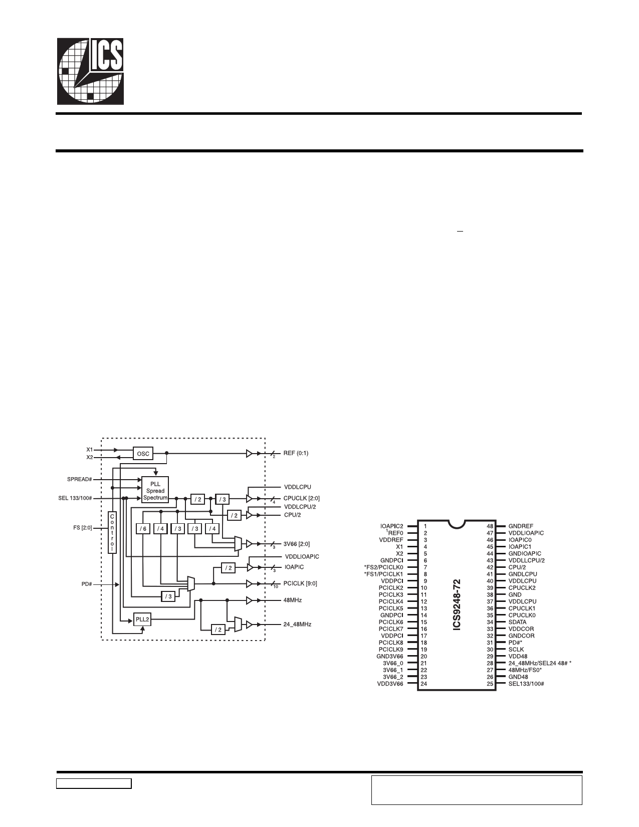
Block Diagram
Features
Up to 200MHz frequency support.
Power Down feature.
Spread Spectrum for EMI control
(0 to 0.5% down spread , + 0.25% center spread)
I2C interface.
VDDL=2.5V,VDD=3.3V
Key Specification
CPU Output Jitter: <250ps
CPU/2 Output Jitter. <250ps
IOAPIC Output Jitter: <500ps
48MHz, 3V66, PCI Output Jitter: <500ps
Ref Output Jitter. <1000ps
CPU Output Skew: <175ps
IOAPIC Output Skew <250ps
PCI Output Skew: <500ps
3V66 Output Skew <250ps
CPU to 3V66 Output Offset: 0.0 - 1.5ns (CPU leads)
3V66 to PCI Output Offset: 1.5 - 4.0ns (3V66 leads)
CPU to IOAPIC Output Offset 1.5 - 4.0ns (CPU leads)
Pin Configuration
9248-72 Rev B 7/28/99
48-pin SSOP
* 250K ohm pull-up to VDD on indicated inputs.
1.These pins will have 2X drive strength
PRODUCT PREVIEW documents contain information on new
products in the sampling or preproduction phase of development.
Characteristic data and other specifications are subject to change
without notice.
1 page 
ICS9248-72
Preliminary Product Preview
Serial Configuration Command Bitmap
Byte0: Functionality and Frequency Select Register (default = 0)
Bit Description
Bit
CPUCLK CPU/2
7 6 54
3V66
1 1 1 1 133.30
66.65
66.65
1 1 1 0 138.01
69.01
69.01
1 1 0 1 142.91
71.45
71.45
1 1 0 0 147.95
73.98
73.98
1 0 1 1 152.49
76.24
76.24
1 0 1 0 156.99
78.49
78.49
Bit
(7:4)
1 0 0 1 162.02
1 0 0 0 180.00
81.01
89.99
81.01
60.00
0 1 1 1 100.23
50.11
66.81
0 1 1 0 105.00
52.49
70.00
0 1 0 1 113.99
56.99
75.66
0 1 0 0 120.00
59.99
80.00
0 0 1 1 128.51
64.25
64.25
0 0 1 0 200.01
100.00
66.66
0 0 0 1 170.03
85.01
56.66
0 0 0 0 66.82
33.40
66.80
Bit3
0-Frequency is selected by hardware select, latched inputs
1- Frequency is selected by Bit 7:4
Bit2
0- Spread spectrum center spread type ±0.25%
1- Spread spectrum down spread type 0 to - 0.5%
Bit1
0- Normal
1- Spread spectrum enable
Bit0
0= Running
1= Tristate all outputs
PCICLK
33.325
34.505
35.725
36.99
38.12
39.245
40.505
30.00
33.405
35
37.83
40.00
32.125
33.33
28.33
33.40
Note1: Default at power-up will be for latched logic inputs to define frequency.
IOAPIC
16.66
17.25
17.86
18.49
19.06
19.62
20.25
15.00
16.70
17.50
18.91
20.00
16.06
16.66
14.16
16.7
PWD
0
XXXX
Note1
0
1
1
0
5
5 Page 
ICS9248-72
Preliminary Product Preview
Electrical Characteristics - 48M, REF
TA = 0 - 70C; VDD = VDDL = 3.3 V +/-5%; CL = 10 -20 pF (unless otherwise stated)
PARAMETER SYMBOL
CONDITIONS
MIN TYP MAX UNITS
Output Impedance
Output Impedance
RDSP51
RDSN51
VO = VDD*(0.5)
VO = VDD*(0.5)
20 60 Ω
20 60 Ω
Output High Voltage VOH5 IOH = 1 mA
2.4 V
Output Low Voltage
VOL5 IOL = -1 mA
0.4 V
Output High Current
IOH5 VOH@MIN=1 V, VOH@MAX= 3.135 V
-29
-23 mA
Output Low Current
Duty Cycle
Jitter
IOL5
dt51
tjcyc-cyc1
tjcyc-cyc1
VOL@MIN=1.95 V, VOL@MIN=0.4 V
VT = 1.5 V
VT = 1.5 V; Fixed Clocks
VT = 1.5 V; Ref Clocks
29 27 mA
45 55 %
500 ps
1000 ps
Skew
Tsk VT = 1.5 V,Fixed Clocks
N/A ps
1Guarenteed by design, not 100% tested in production.
Electrical Characteristics - IOAPIC
TA = 0 - 70C, VDDL = 2.5 V +/-5%; CL = 40 pF (unless otherwise stated)
PARAMETER SYMBOL
CONDITIONS
Output Impedance
RDSP2B1 VO = VDD*(0.5)
Output High Voltage VOH2B IOH = -1 mA
Output Low Voltage VOL2B IOL = 1 mA
Output High Current
IOH2B VOH @MIN= 1.0V , VOH@ MAX= 2.375V
Output Low Current
Rise Time
Fall Time
IOL2B
tr2B1
tf2B1
VOL @MIN= 1.2V , VOL@ MAX= 0.3V
VOL = 0.4 V, VOH = 2.0 V
VOH = 0.4 V, VOL = 2.0 V
Duty Cycle
Skew
Jitter
dt2B1
tsk2B1
tjcyc-cyc1
VT = 1.25 V
VT = 1.25 V
VT = 1.25 V
1Guarenteed by design, not 100% tested in production.
MIN TYP MAX UNITS
13.5 45 Ω
2V
0.4 V
-27 -27 mA
27 30 mA
0.4 1.6 ns
0.4 1.6 ns
45 55 ns
250 ps
500 ps
11
11 Page | ||
| Páginas | Total 12 Páginas | |
| PDF Descargar | [ Datasheet ICS9248-72.PDF ] | |
Hoja de datos destacado
| Número de pieza | Descripción | Fabricantes |
| ICS9248-72 | Frequency Generator & Integrated Buffers | Integrated Circuit Systems |
| ICS9248-73 | Frequency Generator & Integrated Buffers | Integrated Circuit Systems |
| ICS9248-77 | Frequency Generator & Integrated Buffers | Integrated Circuit Systems |
| ICS9248-78 | Frequency Generator & Integrated Buffers | Integrated Circuit Systems |
| Número de pieza | Descripción | Fabricantes |
| SLA6805M | High Voltage 3 phase Motor Driver IC. |
Sanken |
| SDC1742 | 12- and 14-Bit Hybrid Synchro / Resolver-to-Digital Converters. |
Analog Devices |
|
DataSheet.es es una pagina web que funciona como un repositorio de manuales o hoja de datos de muchos de los productos más populares, |
| DataSheet.es | 2020 | Privacy Policy | Contacto | Buscar |