|
|
|
PDF ICS9248-138 Data sheet ( Hoja de datos )
| Número de pieza | ICS9248-138 | |
| Descripción | Frequency Generator & Integrated Buffers | |
| Fabricantes | Integrated Circuit Systems | |
| Logotipo | ||
Hay una vista previa y un enlace de descarga de ICS9248-138 (archivo pdf) en la parte inferior de esta página. Total 12 Páginas | ||
|
No Preview Available !
Integrated
Circuit
Systems, Inc.
ICS9248-138
Preliminary Product Preview
Frequency Generator & Integrated Buffers for Celeron & PII/III™
Recommended Application:
810/810E and Solano type chipset.
Output Features:
• 2- CPUs @ 2.5V
• 9 - SDRAM @ 3.3V, including 1 free running
• 7 - PCICLK @ 3.3V
• 1 - IOAPIC @ 2.5V,
• 3 - 3V66MHz @ 3.3V
• 2 - 48MHz, @ 3.3V fixed.
• 1 - 24/48MHz, @3.3V selectable by I2C
• 1 - REF @v3.3V, 14.318MHz.
Features:
• Up to 200MHz frequency support
• Support FS0-FS4 strapping status bit for I2C read back.
• Support power management: Through Power down
Mode from I2C programming.
• Spread spectrum for EMI control ( ± 0.25% center).
• Uses external 14.318MHz crystal
Skew Specifications:
• CPU – CPU: <175ps
• SDRAM - SDRAM: < 250ps
• 3V66 – 3V66: <175ps
• PCI – PCI: <500ps
• For group skew specifications, please refer to group
timing relationship.
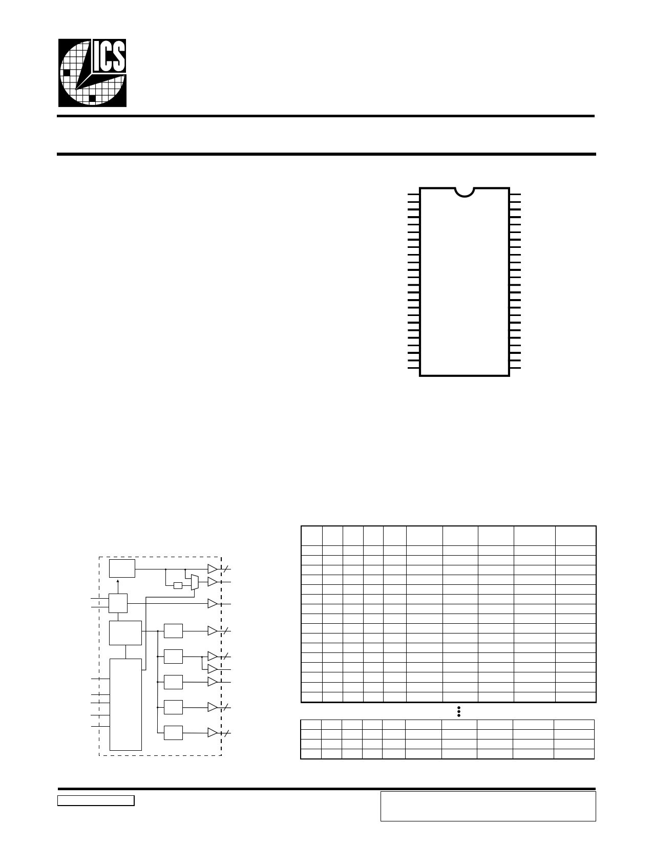
Pin Configuration
1*SEL24_48#/REF0
VDDREF
X1
X2
GNDREF
GND3V66
3V66-0
3V66-1
3V66-2
VDD3V66
VDDPCI
1*FS0/PCICLK0
1**FS1/PCICLK1
GNDPCI
PCICLK2
PCICLK3
PCICLK4
VDDPCI
PCICLK5
PCICLK6
GNDPCI
PD#
SCLK
SDATA
1
2
3
4
5
6
7
8
9
10
11
12
13
14
15
16
17
18
19
20
21
22
23
24
48 VDDLAPIC
47 IOAPIC1
46 VDDLCPU
45 CPUCLK0
44 CPUCLK1
43 GNDLCPU
42 GNDSDR
41 SDRAM0
40 SDRAM1
39 SDRAM2
38 VDDSDR
37 SDRAM3
36 SDRAM4
35 SDRAM5
34 GNDSDR
33 SDRAM6
32 SDRAM7
31 SDRAM_F
30 VDDSDR
29 GND48
28 24_48MHz/FS2**
27 48MHz/FS3*
26 48MHz/FS4*1
25 VDD48
48-Pin 300mil SSOP
* These inputs have a 120K pull up to VDD.
* * These inputs have a 120K pull down to GND.
1 These are double strength.
Block Diagram
PLL2
X1 XTAL
X2 OSC
PLL1
Spread
Spectrum
SEL24_48#
SDATA
SCLK
FS[4:0]
PD#
Control
Logic
Config.
Reg.
/2
CPU
DIVDER
SDRAM
DIVDER
IOAPIC
DIVDER
PCI
DIVDER
3V66
DIVDER
48MHz [1:0]
2
24_48MHz
REF0
CPUCLK [1:0]
2
SDRAM [7:0]
8
SDRAM_F
IOAPIC
PCICLK [6:0]
7
3V66 [2:0]
3
9248- 138 Rev A 10/03/00
Third party brands and names are the property of their respective owners.
Functionality
FS4 FS3 FS2 FS1 FS0
0000 0
0000 1
00010
0001 1
0 0 10 0
0 0 10 1
00 110
00 11 1
0 100 0
0 100 1
0 10 1 0
0 10 1 1
0 1 10 0
0 1 10 1
0 1110
0 111 1
CPU
(MHz)
66.67
66.87
68.67
71.34
100.00
100.30
103.00
107.00
133.33
133.73
137.33
120.00
133.33
133.73
137.33
120.00
SDRAM
(MHz)
100.00
100.30
103.00
107.00
100.00
100.30
103.00
107.00
133.33
133.73
137.33
120.00
100.00
100.30
103.00
90.00
3V66
(MHz)
66.67
66.87
68.67
71.34
66.67
66.87
68.67
71.34
66.67
66.87
68.67
60.00
66.67
66.87
68.67
60.00
PCICLK
(MHz)
33.33
33.43
34.33
35.66
33.33
33.43
34.33
35.66
33.33
33.43
34.33
30.00
33.33
33.43
34.33
30.00
IOAPIC
(MHz)
16.67
16.72
17.16
17.83
16.67
16.72
17.17
17.84
16.67
16.72
17.17
15.00
16.67
16.72
17.17
15.00
1 1 0 1 0 160.00 160.00 80.00
1 1 1 0 1 160.00 120.00 80.00
1 1 0 1 1 166.67 166.67 83.34
1 1 1 1 0 166.67 125.00 83.34
40.00
40.00
41.67
41.67
20.00
20.00
20.84
20.84
Additional frequencies selectable through I2C programming.
PRODUCT PREVIEW documents contain information on new
products in the sampling or preproduction phase of development.
Characteristic data and other specifications are subject to change
without notice.
1 page 
ICS9248-138
Preliminary Product Preview
Absolute Maximum Ratings
Core Supply Voltage . . . . . . . . . . . . . . . . . . . . . . . 5.5 V
I/O Supply Voltage . . . . . . . . . . . . . . . . . . . . . . . . . 3.6V
Logic Inputs . . . . . . . . . . . . . . . . . . . . . . . . . . . . . . GND 0.5 V to VDD +0.5 V
Ambient Operating Temperature . . . . . . . . . . . . . 0°C to +70°C
Storage Temperature . . . . . . . . . . . . . . . . . . . . . . . 65°C to +150°C
Stresses above those listed under Absolute Maximum Ratings may cause permanent damage to the device. These ratings are
stress specifications only and functional operation of the device at these or any other conditions above those listed in the
operational sections of the specifications is not implied. Exposure to absolute maximum rating conditions for extended periods
may affect product reliability.
Group Timing Relationship Table
Group
CPU to SDRAM
CPU to 3V66
CPU 66MHz
SDRAM 100MHz
Offset Tolerance
2.5ns 500ps
7.5ns 500ps
CPU 100MHz
SDRAM 100MHz
Offset Tolerance
5.0ns 500ps
5.0ns 500ps
CPU 133MHz
SDRAM 100MHz
Offset Tolerance
0.0ns 500ps
0.0ns 500ps
CPU 133MHz
SDRAM 133MHz
Offset Tolerance
3.75ns 500ps
0.0ns 500ps
SDRAM to 3V66 0.0ns 500ps 0.0ns 500ps 0.0ns 500ps 3.75ns 500ps
3V66 to PCI
PCI to PCI
USB & DOT
1.5-3.5ns
0.0ns
Asynch
500ps
1.0ns
N/A
1.5-3.5ns
0.0ns
Asynch
500ps
1.0ns
N/A
1.5-3.5ns
0.0ns
Asynch
500ps
1.0ns
N/A
1.5 -3.5ns
0.0ns
Asynch
500ps
1.0ns
N/A
Electrical Characteristics - Input/Supply/Common Output Parameters
TA = 0 - 70C; Supply Voltage VDD = 3.3 V +5%, VDDL=2.5 V+ 5%(unless otherwise stated)
PARAMETER
SYMBOL
CONDITIONS
MIN TYP MAX UNITS
Input High Voltage
Input Low Voltage
Input High Current
Input Low Current
Input Low Current
Operating
Supply Current
Power Down
Supply Current
VIH
VIL
IIH
IIL1
IIL2
IDD3.3OP
VIN = VDD
VIN = 0 V; Inputs with no pull-up resistors
VIN = 0 V; Inputs with pull-up resistors
CL = 0 pF; Select @ 66M
2
VSS-0.3
-5
-5
-200
IDD3.3PD CL = 0 pF; With input address to Vdd or GND
VDD+0.3
0.8
5
100
V
V
µA
µA
µA
mA
600 µA
Input frequency
Fi VDD = 3.3 V;
Pin Inductance
Input Capacitance1
Lpin
CIN Logic Inputs
Cout Out put pin capacitance
Transition Time1
Settling Time1
Clk Stabilization1
CINX
Ttrans
Ts
TSTAB
X1 & X2 pins
To 1st crossing of target Freq.
From 1st crossing to 1% target Freq.
From VDD = 3.3 V to 1% target Freq.
Delay
tPZH,tPZH output enable delay (all outputs)
tPLZ,tPZH output disable delay (all outputs)
1Guarenteed by design, not 100% tested in production.
14.318
7
5
6
27 45
3
3
3
1 10
1 10
MHz
nH
pF
pF
pF
mS
mS
mS
nS
nS
Third party brands and names are the property of their respective owners.
5
5 Page 
ICS9248-138
Preliminary Product Preview
PD# Timing Diagram
The power down selection is used to put the part into a very low power state without turning off the power to the part. PD# is
an asynchronous active low input. This signal needs to be synchronized internal to the device prior to powering down the clock
synthesizer.
Internal clocks are not running after the device is put in power down. When PD# is active low all clocks need to be driven to a
low value and held prior to turning off the VCOs and crystal. The power up latency needs to be less than 3 mS. The power down
latency should be as short as possible but conforming to the sequence requirements shown below. The REF and 48MHz clocks
are expected to be stopped in the LOW state as soon as possible. Due to the state of the internal logic, stopping and holding
the REF clock outputs in the LOW state may require more than one clock cycle to complete.
PD#
CPUCLK
3V66
PCICLK
VCO
Crystal
Notes:
1. All timing is referenced to the Internal CPUCLK (defined as inside the ICS9248 device).
2. As shown, the outputs Stop Low on the next falling edge after PD# goes low.
3. PD# is an asynchronous input and metastable conditions may exist. This signal is synchronized inside this part.
4. The shaded sections on the VCO and the Crystal signals indicate an active clock.
5. Diagrams shown with respect to 133MHz. Similar operation when CPU is 100MHz.
Third party brands and names are the property of their respective owners.
11
11 Page | ||
| Páginas | Total 12 Páginas | |
| PDF Descargar | [ Datasheet ICS9248-138.PDF ] | |
Hoja de datos destacado
| Número de pieza | Descripción | Fabricantes |
| ICS9248-131 | Frequency Generator & Integrated Buffers | Integrated Circuit Systems |
| ICS9248-134 | Frequency Generator & Integrated Buffers | Integrated Circuit Systems |
| ICS9248-135 | Frequency Generator & Integrated Buffers | Integrated Circuit Systems |
| ICS9248-136 | Frequency Generator & Integrated Buffers | Integrated Circuit Systems |
| Número de pieza | Descripción | Fabricantes |
| SLA6805M | High Voltage 3 phase Motor Driver IC. |
Sanken |
| SDC1742 | 12- and 14-Bit Hybrid Synchro / Resolver-to-Digital Converters. |
Analog Devices |
|
DataSheet.es es una pagina web que funciona como un repositorio de manuales o hoja de datos de muchos de los productos más populares, |
| DataSheet.es | 2020 | Privacy Policy | Contacto | Buscar |