|
|
|
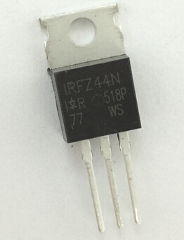
PDF IRFZ44N Data sheet ( Hoja de datos )
| Número de pieza | IRFZ44N | |
| Descripción | 49A, 55V, N-channel Enhancement Mode TrenchMOS Transistor | |
| Fabricantes | NXP Semiconductors | |
| Logotipo | ||
 1. - IR ( PDF ) Hay una vista previa y un enlace de descarga de IRFZ44N (archivo pdf) en la parte inferior de esta página. Total 8 Páginas | ||
|
No Preview Available !
www.DataSheet4U.com
Philips Semiconductors
N-channel enhancement mode
TrenchMOSTM transistor
Product specification
IRFZ44N
GENERAL DESCRIPTION
N-channel enhancement mode
standard level field-effect power
transistor in a plastic envelope using
’trench’ technology. The device
features very low on-state resistance
and has integral zener diodes giving
ESD protection up to 2kV. It is
intended for use in switched mode
power supplies and general purpose
switching applications.
QUICK REFERENCE DATA
SYMBOL PARAMETER
VDS
ID
Ptot
Tj
RDS(ON)
Drain-source voltage
Drain current (DC)
Total power dissipation
Junction temperature
Drain-source on-state
resistance
VGS = 10 V
MAX.
55
49
110
175
22
PINNING - TO220AB
PIN DESCRIPTION
1 gate
2 drain
3 source
tab drain
PIN CONFIGURATION
tab
1 23
SYMBOL
d
g
s
UNIT
V
A
W
˚C
mΩ
LIMITING VALUES
Limiting values in accordance with the Absolute Maximum System (IEC 134)
SYMBOL PARAMETER
CONDITIONS
VDS
VDGR
±VGS
ID
ID
IDM
Ptot
Tstg, Tj
Drain-source voltage
Drain-gate voltage
Gate-source voltage
Drain current (DC)
Drain current (DC)
Drain current (pulse peak value)
Total power dissipation
Storage & operating temperature
-
RGS = 20 kΩ
-
Tmb = 25 ˚C
Tmb = 100 ˚C
Tmb = 25 ˚C
Tmb = 25 ˚C
-
ESD LIMITING VALUE
SYMBOL
VC
PARAMETER
Electrostatic discharge capacitor
voltage, all pins
CONDITIONS
Human body model
(100 pF, 1.5 kΩ)
THERMAL RESISTANCES
SYMBOL
Rth j-mb
Rth j-a
PARAMETER
Thermal resistance junction to
mounting base
Thermal resistance junction to
ambient
CONDITIONS
-
in free air
MIN.
-
-
-
-
-
-
-
- 55
MAX.
55
55
20
49
35
160
110
175
UNIT
V
V
V
A
A
A
W
˚C
MIN.
-
MAX.
2
UNIT
kV
TYP.
-
60
MAX.
1.4
-
UNIT
K/W
K/W
February 1999
DataSheet4 U .com
1
Rev 1.000
1 page 
www.DataSheet4U.com
Philips Semiconductors
N-channel enhancement mode
TrenchMOSTM transistor
Product specification
IRFZ44N
1E-01
Sub-Threshold Conduction
1E-02
1E-03
2% typ
98%
1E-04
1E-05
1E-06
01234
Fig.11. Sub-threshold drain current.
ID = f(VGS); conditions: Tj = 25 ˚C; VDS = VGS
5
2.5
2
1.5
Ciss
1
.5
0
0.01 0.1
1 VDS/V 10
Coss
Crss
100
Fig.12. Typical capacitances, Ciss, Coss, Crss.
C = f(VDS); conditions: VGS = 0 V; f = 1 MHz
12
VGS/V
10
8
6
VDS = 14V
VDS = 44V
4
2
0
0 10 20 QG/nC 30 40 50
Fig.13. Typical turn-on gate-charge characteristics.
VGS = f(QG); conditions: ID = 50 A; parameter VDS
100
IF/A
80
60
Tj/C =
175
25
40
20
0
0 0.2 0.4 0.6 0.8 1 1.2 1.4
VSDS/V
Fig.14. Typical reverse diode current.
IF = f(VSDS); conditions: VGS = 0 V; parameter Tj
WDSS%
120
110
100
90
80
70
60
50
40
30
20
10
0
20 40 60 80 100 120 140 160 180
Tmb / C
Fig.15. Normalised avalanche energy rating.
WDSS% = f(Tmb); conditions: ID = 49 A
VGS
0
RGS
L
VDS
T.U.T.
+ VDD
-
-ID/100
R 01
shunt
Fig.16. Avalanche energy test circuit.
WDSS = 0.5 ⋅ LID2 ⋅ BVDSS/(BVDSS − VDD)
February 1999
DataSheet4 U .com
5
Rev 1.000
5 Page | ||

| Páginas | Total 8 Páginas | |
| PDF Descargar | [ Datasheet IRFZ44N.PDF ] | |
Hoja de datos destacado
| Número de pieza | Descripción | Fabricantes |
| IRFZ44 | Power MOSFET ( Transistor ) | IR |
| IRFZ44 | (IRFZ40 - IRFZ45) N-Channel Power MOSFETS | Samsung Electronics |
| IRFZ44 | Power MOSFET ( Transistor ) | Fairchild |
| IRFZ44 | Power MOSFET ( Transistor ) | Vishay |
| Número de pieza | Descripción | Fabricantes |
| SLA6805M | High Voltage 3 phase Motor Driver IC. |
Sanken |
| SDC1742 | 12- and 14-Bit Hybrid Synchro / Resolver-to-Digital Converters. |
Analog Devices |
|
DataSheet.es es una pagina web que funciona como un repositorio de manuales o hoja de datos de muchos de los productos más populares, |
| DataSheet.es | 2020 | Privacy Policy | Contacto | Buscar |