|
|
|
PDF CDS-1402 Data sheet ( Hoja de datos )
| Número de pieza | CDS-1402 | |
| Descripción | 14-Bit / Very Fast Settling Correlated Double Sampling Circuit | |
| Fabricantes | ETC | |
| Logotipo | ||
Hay una vista previa y un enlace de descarga de CDS-1402 (archivo pdf) en la parte inferior de esta página. Total 8 Páginas | ||
|
No Preview Available !
®®
CDS-1402
14-Bit, Very Fast Settling
Correlated Double Sampling Circuit
FEATURES
• Use with 10 to 14-bit A/D converters
• 5 Megapixels/second minimum throughput (14 bits)
• ±2.5V input/output ranges, Gain = –1
• Low noise, 200µVrms
• Two independent S/H amplifiers
• Gain matching between S/H's
• Offset adjustments for each S/H
• Four external A/D control lines
• Small package, 24-pin ceramic DDIP
• Low power, 350mW
• Low cost
GENERAL DESCRIPTION
The CDS-1402 is an application-specific, correlated double
sampling (CDS) circuit designed for electronic-imaging
applications that employ CCD's (charge coupled devices) as
their photodetector. The CDS-1402 has been optimized for
use in digital video applications that employ 10 to 14-bit A/D
converters. The low-noise CDS-1402 can accurately
determine each pixel's true video signal level by sequentially
sampling the pixel's offset signal and its video signal and
subtracting the two. The result is that the consequences of
residual charge, charge injection and low-frequency "kTC"
noise on the CCD's output floating capacitor are effectively
eliminated. The CDS-1402 can also be used as a dual
sample-hold amplifier in a data acquisition system.
The CDS-1402 contains two sample-hold amplifiers and
appropriate support/control circuitry. Features include
independent offset-adjust capability for each S/H,
adjustment for matching gain between the two S/H's,
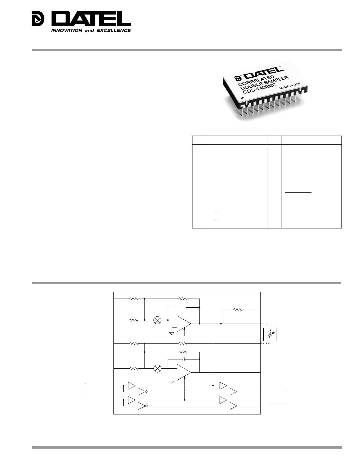
INPUT/OUTPUT CONNECTIONS
PIN FUNCTION
PIN FUNCTION
1 OFFSET ADJUST V1
2 DO NOT CONNECT
3 ANALOG INPUT 1
4 ANALOG INPUT 2
5 ANALOG GROUND
6 S/H1 OUT
7 S/H1 ROUT
8 S/H2 SUMMING NODE
9 OFFSET ADJUST V2
10 DO NOT CONNECT
11 S/H1 COMMAND
12 S/H2 COMMAND
24 +5V ANALOG SUPPLY
23 ANALOG GROUND
22 V OUT
21 ANALOG GROUND
20 A/D CLOCK2
19 A/D CLOCK2
18 A/D CLOCK1
17 A/D CLOCK1
16 +5V DIGITAL SUPPLY
15 DIGITAL GROUND
14 ANALOG GROUND
13 –5V ANALOG SUPPLY
and four control lines for triggering the A/D converter used in
conjunction with the CDS-1402. The CDS circuit's "ping-
pong" timing approach (the offset signal of the "n+1" pixel can
be acquired while the video output of the "nth" pixel is being
converted) guarantees a minimum throughput, in a 14-bit
application, of 5MHz. In other words, the true video signal
(minus offset) will be available
(continued on page 3)
OFFSET ADJUST V1 1
DO NOT CONNECT 2
ANALOG INPUT 1 3
OFFSET ADJUST V2 9
DO NOT CONNECT 10
ANALOG INPUT 2 4
S/H1 COMMAND 11
S/H2 COMMAND 12
100kΩ
500Ω
100kΩ
500Ω
500Ω
CH
–
S/H 1
+
450Ω
500Ω
CH
–
S/H 2
+
50Ω
7 S/H1 ROUT
6 S/H1 OUT
OPTIONAL
8 S/H2
SUMMING NODE
22 V OUT
18 A/D CLOCK 1
17 A/D CLOCK 1
19 A/D CLOCK 2
20 A/D CLOCK 2
5, 14, 21, 23
ANALOG GROUND
24
+5V ANALOG
SUPPLY
13
–5V ANALOG
SUPPLY
16
+5V DIGITAL
SUPPLY
15
DIGITAL
GROUND
Figure 1. CDS-1402 Functional Block Diagram
DATEL, Inc., 11 Cabot Boulevard, Mansfield, MA 02048-1151 (U.S.A.) • Tel: (508) 339-3000 Fax: (508) 339-6356 • For immediate assistance: (800) 233-2765
1 page 
®®
CDS-1402
package so they can be used to control other circuit functions.
Each S/H has two pins for offset adjusting (if required), one for
current and one for voltage.
In normal operation, the output signal of the CCD is applied
simultaneously to the inputs (pins 3 and 4) of both S/H
amplifiers. S/H1 will normally be used to capture and hold
each pixel’s offset signal. Therefore, S/H1 is initially in its
signal-acquisition mode (logic "1" applied to pin 11, S/H1
COMMAND). This is also called the sample or track mode.
Following a brief interval during which the output of the CCD
and the output of S/H1 are allowed to settle, S/H1 is driven into
its hold mode by applying a logic "0" to pin 11. S/H1 is now
holding the pixel's offset value.
In most straightforward configurations, the output of S/H1 is
connected to the summing node of S/H2 by connecting pin 7
(S/H1 ROUT) to pin 8 (S/H2 SUMMING NODE).
When the offset+video signal appears at the output of the CCD,
S/H2 is driven into its signal acquisition mode by applying a
logic "1" to pin 12 (S/H2 COMMAND).
S/H2 employs a current-summing architecture that subtracts
the output of S/H1 (the offset) from the output of the CCD
(offset+video) while acquiring only the difference signal (i.e.,
the valid video). A logic "0" subsequently applied to pin 12
drives S/H2 into its hold mode, and after a brief transient
settling time, the valid video signal appears at pin 22 (V OUT).
Timing Notes
See Figure 2, Typical Timing Diagram. It is advisable that
neither of the CDS-1402's S/H amplifiers be in their sample/
track mode when large, high-speed transients (normally
associated with clock edges) are occurring throughout the
system. This could result in the S/H amplifiers being driven
into saturation, and they may not recover in time to accurately
acquire their next signal.
For example, S/H1 should not be commanded into the sample
mode until all transients associated with the opening of the
shunt switch have begun to decay. Similarly, S/H2 should not
be driven into the sample mode until all transients associated
with the clocking of pixel charge onto the output capacitor
have begun to decay. Therefore, it is generally not a good
practice to use the same clock edge to drive S/H1 into hold
(holding the offset) and S/H2 into sample (to acquire the offset
+ video signal).
S/H's that are in their signal-acquisition modes should be left
there as long as possible (so all signals can settle) and be
driven into their hold modes before any system transients
occur. In Figure 2, S/H1 is driven into the sample mode
shortly after the transient from the shunt switch has begun to
decay. S/H1 is then kept in the sample mode while the offset
signal and the S/H output settle. S/H1 is driven into hold just
prior to the system clock pulse(s) that transfers the next pixel
charge onto the output capacitor.
(CCD OUTPUT)
ANALOG INPUT
FOR CDS
(Pins 3 and 4 are tied together)
S/H1
S/H2
START CONVERT
EOC
OUTPUT
DATA
OFFSET (N+1)
OFFSET +
VIDEO (N+1)
OFFSET (N+2)
100ns
30ns typ.
100ns
35ns typ.
150ns
DATA N-1 VALID
10ns min.
50ns max.
DATA N VALID
Figure 3. CDS-1402 in Front of DATEL's ADC-944 at fCLK = 4MHz
OFFSET +
VIDEO (N+2)
DATA N+1 VALID
5
5 Page | ||
| Páginas | Total 8 Páginas | |
| PDF Descargar | [ Datasheet CDS-1402.PDF ] | |
Hoja de datos destacado
| Número de pieza | Descripción | Fabricantes |
| CDS-1402 | 14-Bit / Very Fast Settling Correlated Double Sampling Circuit | ETC |
| Número de pieza | Descripción | Fabricantes |
| SLA6805M | High Voltage 3 phase Motor Driver IC. |
Sanken |
| SDC1742 | 12- and 14-Bit Hybrid Synchro / Resolver-to-Digital Converters. |
Analog Devices |
|
DataSheet.es es una pagina web que funciona como un repositorio de manuales o hoja de datos de muchos de los productos más populares, |
| DataSheet.es | 2020 | Privacy Policy | Contacto | Buscar |