|
|
|
PDF LM3310 Data sheet ( Hoja de datos )
| Número de pieza | LM3310 | |
| Descripción | Step-up PWM DC/DC Converter with Integrated Op-Amp and Gate Pulse Modulation Switch | |
| Fabricantes | National Semiconductor | |
| Logotipo | ||
Hay una vista previa y un enlace de descarga de LM3310 (archivo pdf) en la parte inferior de esta página. Total 25 Páginas | ||
|
No Preview Available !
August 2005
LM3310
Step-up PWM DC/DC Converter with Integrated Op-Amp
and Gate Pulse Modulation Switch
General Description
The LM3310 is a step-up DC/DC converter integrated with
an Operational Amplifier and a gate pulse modulation switch.
The boost (step-up) converter is used to generate an adjust-
able output voltage and features a low RDSON internal switch
for maximum efficiency. The operating frequency is select-
able between 660kHz and 1.28MHz allowing for the use of
small external components. An external soft-start pin en-
ables the user to tailor the soft-start time to a specific appli-
cation and limit the inrush current. The Op-Amp is capable of
sourcing/sinking 135mA of current (typical). The gate pulse
modulation switch can operate with a VGH voltage of 5V to
30V. The LM3310 is available in a low profile 24-lead LLP
package.
Features
n Boost converter with a 2A, 0.18Ω switch
n Boost output voltage adjustable up to 20V
n Operating voltage range of 2.5V to 7V
n 660kHz/1.28MHz pin selectable switching frequency
n Adjustable soft-start function
n Input undervoltage protection
n Over temperature protection
n Integrated Op-Amp
n Integrated gate pulse modulation (GPM) switch
n 24-Lead LLP package
Applications
n TFT Bias Supplies
n Portable Applications
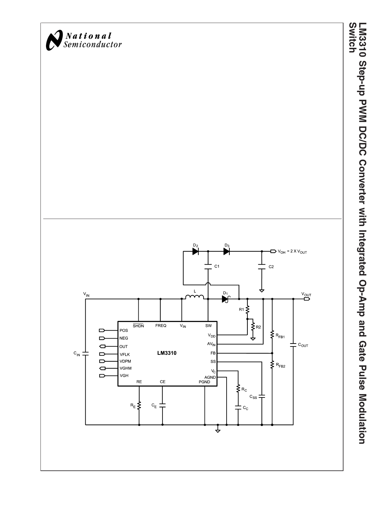
Typical Application Circuit
© 2005 National Semiconductor Corporation DS201333
20133331
www.national.com
1 page 
Absolute Maximum Ratings (Note 1)
If Military/Aerospace specified devices are required,
please contact the National Semiconductor Sales Office/
Distributors for availability and specifications.
VIN
SW Voltage
FB Voltage
VC Voltage (Note 2)
SHDN Voltage
FREQ
AVIN
Amplifier Inputs/Output
VGH Voltage
VGHM Voltage
VFLK, VDPM, VDD Voltage
CE Voltage (Note 2)
RE Voltage
Maximum Junction
Temperature
7.5V
21V
VIN
1.265V ± 0.3V
7.5V
VIN
12V
Rail-to-Rail
31V
VGH
7.5V
1.265 + 0.3V
VGH
150˚C
Power Dissipation(Note 3)
Lead Temperature
Vapor Phase (60 sec.)
Infrared (15 sec.)
ESD Susceptibility (Note 4)
Human Body Model
Internally Limited
300˚C
215˚C
220˚C
2kV
Operating Conditions
Operating Junction
Temperature Range (Note 5)
Storage Temperature
Supply Voltage
Maximum SW Voltage
VGH Voltage Range
Op-Amp Supply, AVIN
−40˚C to +125˚C
−65˚C to +150˚C
2.5V to 7V
20V
5V to 30V
4V to 12V
Electrical Characteristics VIN =2.5V and IL = 0A
Specifications in standard type face are for TJ = 25˚C and those with boldface type apply over the full Operating Tempera-
ture Range ( TJ = −40˚C to +125˚C). Unless otherwise specified, VIN =2.5V and IL = 0A.
Symbol
Parameter
Conditions
Min(Note 5) Typ(Note 6) Max(Note 5) Units
IQ Quiescent Current
FB = 2V (Not Switching)
VSHDN = 0V
690
0.04
1100
0.5
8.5
µA
660kHz Switching
1.28MHz Switching
2.1 2.8
mA
3.1 4.0
VFB
%VFB/∆VIN
Feedback Voltage
Feedback Voltage Line
Regulation
2.5V ≤ VIN ≤ 7V
1.231
-0.26
1.263
0.089
1.287
0.42
V
%/V
ICL
IB
ISS
VSS
VIN
gm
AV
DMAX
fS
ISHDN
IL
RDSON
ThSHDN
Switch Current Limit (Note 7) (Note 8)
FB Pin Bias Current (Note 9)
SS Pin Current
SS Pin Voltage
Input Voltage Range
Error Amp Transconductance ∆I = 5µA
Error Amp Voltage Gain
Maximum Duty Cycle
Switching Frequency
fS = 660kHz
fS = 1.28MHz
FREQ = Ground
Shutdown Pin Current
Switch Leakage Current
Switch RDSON
SHDN Threshold
FREQ = VIN
VSHDN = 2.5V
VSHDN = 0.3V
VSW = 20V
ISW = 500mA
Output High, VIN = 2.5V to
7V
2.0
8.5
1.20
2.5
26
80
80
440
1.0
1.4
2.6
27
11
1.24
74
69
91
89
660
1.28
8
1
0.03
0.18
160
13.5
1.28
7
133
A
nA
µA
V
V
µmho
V/V
%
760
1.5
13.5
2
5
0.35
kHz
MHz
µA
µA
Ω
V
Output Low, VIN = 2.5V to 7V
0.4
UVP
Undervoltage Protection
On Threshold (Switch On)
2.5
2.4
Threshold
Off Threshold (Switch Off)
2.3 2.1
V
5 www.national.com
5 Page 
Typical Performance Characteristics (Continued)
1.28MHz Max. Duty Cycle vs. Temperature
1.28MHz Application Efficiency
20133376
1.28MHz Application Efficiency
20133382
VGH Pin Bias Current vs. VGH Pin Voltage
20133326
VGH Pin Bias Current vs. VGH Pin Voltage
20133377
VGH-VGHM PMOS RDSON vs. VGH Pin Voltage
20133378
11
20133379
www.national.com
11 Page | ||
| Páginas | Total 25 Páginas | |
| PDF Descargar | [ Datasheet LM3310.PDF ] | |
Hoja de datos destacado
| Número de pieza | Descripción | Fabricantes |
| LM331 | V-F Converter | Fairchild Semiconductor |
| LM331 | Precision Voltage-to-Frequency Converters | National Semiconductor |
| LM331 | LMx31x Precision Voltage-to-Frequency Converters (Rev. C) | Texas Instruments |
| LM3310 | LM3310 Step-Up PWM DC/DC Converter w/Integrated Op-Amp Gate Pulse Mod Switch (Rev. E) | Texas Instruments |
| Número de pieza | Descripción | Fabricantes |
| SLA6805M | High Voltage 3 phase Motor Driver IC. |
Sanken |
| SDC1742 | 12- and 14-Bit Hybrid Synchro / Resolver-to-Digital Converters. |
Analog Devices |
|
DataSheet.es es una pagina web que funciona como un repositorio de manuales o hoja de datos de muchos de los productos más populares, |
| DataSheet.es | 2020 | Privacy Policy | Contacto | Buscar |