|
|
|
PDF 145406 Data sheet ( Hoja de datos )
| Número de pieza | 145406 | |
| Descripción | MC145406 | |
| Fabricantes | ETC | |
| Logotipo | ||
Hay una vista previa y un enlace de descarga de 145406 (archivo pdf) en la parte inferior de esta página. Total 12 Páginas | ||
|
No Preview Available !
MOTOROLA
SEMICONDUCTOR TECHNICAL DATA
Order this document
by MC145406/D
Driver/Receiver
EIA 232–E and CCITT V.28 (Formerly RS–232–D)
The MC145406 is a silicon–gate CMOS IC that combines three drivers
and three receivers to fulfill the electrical specifications of standards
EIA 232–E and CCITT V.28. The drivers feature true TTL input
compatibility, slew–rate–limited output, 300–Ω power–off source imped-
ance, and output typically switching to within 25% of the supply rails. The
receivers can handle up to ± 25 V while presenting 3 to 7 kΩ impedance.
Hysteresis in the receivers aids reception of noisy signals. By combining
both drivers and receivers in a single CMOS chip, the MC145406 provides
efficient, low–power solutions for EIA 232–E and V.28 applications.
Drivers
• ± 5 V to ±12 V Supply Range
• 300–Ω Power–Off Source Impedance
• Output Current Limiting
• TTL Compatible
• Maximum Slew Rate = 30 V/µs
Receivers
• ± 25 V Input Voltage Range When VDD = 12 V, VSS = – 12 V
• 3 to 7 kΩ Input Impedance
• Hysteresis on Input Switchpoint
MC145406
16
1
16
1
P SUFFIX
PLASTIC
CASE 648
DW SUFFIX
SOG
CASE 751G
SD SUFFIX
SSOP
CASE 940B
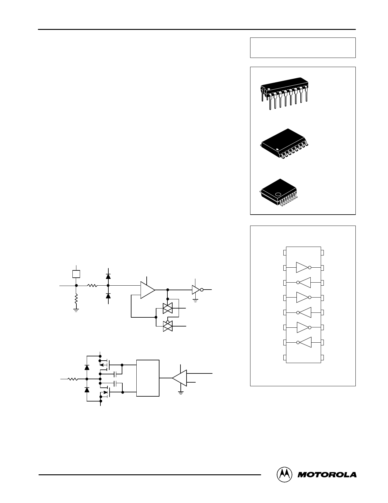
BLOCK DIAGRAM
VDD
RECEIVER
VDD
*
15 kΩ
Rx
VCC
+
–
5.4 k
VSS
VCC
1.0 V
DO
1.8 V
HYSTERESIS
VDD
DRIVER
VCC
300 Ω
Tx
LEVEL
SHIFT
+ DI
– 1.4 V
PIN ASSIGNMENT
VDD 1
16 VCC
Rx1 2 R
15
DO1
3
Tx1
D 14 DI1
Rx2 4 R
13 DO2
Tx2 5
D 12 DI2
6
Rx3
7
Tx3
R 11 DO3
D 10 DI3
VSS 8
9 GND
D = DRIVER
R = RECEIVER
VSS
*Protection circuit
M© OMoTtoOroRla,OInLc.A1995
REV 4
1/95
MC145406
1
1 page 
APPLICATIONS INFORMATION
The MC145406 has been designed to meet the electrical
specifications of standards EIA 232–E and CCITT V.28.
EIA 232–E defines the electrical and physical interface be-
tween Data Communication Equipment (DCE) and Data
Terminal Equipment (DTE). A DCE is connected to a DTE
using a cable that typically carries up to 25 leads. These
leads, referred to as interchange circuits, allow the transfer
of timing, data, control, and test signals. Electrically this
transfer requires level shifting between the TTL/CMOS log-
ic levels of the computer or modem and the high voltage lev-
els of EIA 232–E, which can range from ± 3 to ± 25 V. The
MC145406 provides the necessary level shifting as well as
meeting other aspects of the EIA 232–E specification.
DRIVERS
As defined by the specification, an EIA 232–E driver pres-
ents a voltage of between ± 5 to ± 15 V into a load of be-
tween 3 to 7 kΩ. A logic 1 at the driver input results in a
voltage of between – 5 to – 15 V. A logic 0 results in a voltage
between + 5 to + 15V. When operating VDD and VSS at ± 7 to
± 12 V, the MC145406 meets this requirement. When operat-
ing at ± 5 V, the MC145406 drivers produce less than
± 5 V at the output (when terminated), which does not meet
EIA 232–E specification. However, the output voltages when
using a ± 5 V power supply are high enough (around
± 4 V) to permit proper reception by an EIA 232–E receiver,
and can be used in applications where strict compliance to
EIA 232–E is not required.
Another requirement of the MC145406 drivers is that
they withstand a short to another driver in the EIA 232–E
cable. The worst–case condition that is permitted by
EIA 232–E is a ± 15 V source that is current limited to 500
mA. The MC145406 drivers can withstand this condition
momentarily. In most short circuit conditions the source
driver will have a series 300 Ω output impedance needed
to satisfy the EIA 232–E driver requirements. This will re-
duce the short circuit current to under 40 mA which is an
acceptable level for the MC145406 to withstand.
Unlike some other drivers, the MC145406 drivers feature
an internally–limited output slew–rate that does not exceed
30 V per µs.
RECEIVERS
The job of an EIA 232–E receiver is to level–shift voltages
in the range of – 25 to + 25 V down to TTL/CMOS logic lev-
els (0 to + 5 V). A voltage of between – 3 and – 25 V on Rx1
is defined as a mark and produces a logic 1 at DO1. A volt-
age between + 3 and + 25 V is a space and produces a logic
zero. While receiving these signals, the Rx inputs must pres-
ent a resistance between 3 and 7 kΩ. Nominally, the input re-
sistance of the Rx1–Rx3 inputs is 5.4 kΩ.
The input threshold of the Rx1–Rx3 inputs is typically
biased at 1.8 V above ground (GND) with typically 800 mV of
hysteresis included to improve noise immunity. The 1.8 V
bias forces the appropriate DO pin to a logic 1 when its Rx
input is open or grounded as called for in the EIA 232–E
specification. Notice that TTL logic levels can be applied to
the Rx inputs in lieu of normal EIA 232–E signal levels. This
might be helpful in situations where access to the modem or
computer through the EIA 232–E connector is necessary
with TTL devices. However, it is important not to connect the
EIA 232–E outputs (Tx1–Tx3) to TTL inputs since TTL oper-
ates off + 5 V only, and may be damaged by the high output
voltage of the MC145406.
The DO outputs are to be connected to a TTL or CMOS
input (such as an input to a modem chip). These outputs
will swing from VCC to ground, allowing the designer to op-
erate the DO and DI pins from digital power supply. The Tx
and Rx sections are independently powered by VDD and
VSS so that one may run logic at + 5 V and the EIA 232–E
signals at ± 12 V.
POWER SUPPLY CONSIDERATIONS
Figure 4 shows a technique to guard against excessive
device current.
The diode D1 prevents excessive current from flowing
through an internal diode from the VCC pin to the VDD pin
when VDD < VCC by approximately 0.6 V. This high current
condition can exist for a short period of time during power
up/down. Additionally, if the + 12 V supply is switched off
while the + 5 V is on and the off supply is a low impedance
to ground, the diode D1 will prevent current flow through
the internal diode.
The diode D2 is used as a voltage clamp, to prevent VSS
from drifting positive to VCC, in the event that power is re-
moved from VSS (Pin 12). If VSS power is removed, and the
impedance from the VSS pin to ground is greater than
approximately 3 kΩ, this pin will be pulled to VCC by internal
circuitry causing excessive current in the VCC pin.
If by design, neither of the above conditions are allowed
to exist, then the diodes D1 and D2 are not required.
ESD PROTECTION
ESD protection on IC devices that have their pins accessi-
ble to the outside world is essential. High static voltages ap-
plied to the pins when someone touches them either directly
or indirectly can cause damage to gate oxides and transistor
junctions by coupling a portion of the energy from the I/O pin
to the power supply buses of the IC. This coupling will usually
occur through the internal ESD protection diodes. The key to
protecting the IC is to shunt as much of the energy to ground
as possible before it enters the IC. Figure 4 shows a tech-
nique which will clamp the ESD voltage at approximately ±
15 V using the MMVZ15VDLT1. Any residual voltage which
appears on the supply pins is shunted to ground through the
capacitors C1–C3. This scheme has provided protection to
the interface part up to ± 10 kV, using the human body model
test.
MOTOROLA
MC145406
5
5 Page 
SD SUFFIX
CASE 940B–02
16 8
B
-R-
17
A
-P-
-T-
H
G
D
0.120 (0.005) M T P S
L
0.250 (0.010) M R M
JM
F
NOTE 4
C
N 0.076 (0.003)
NOTES:
1. DIMENSIONING AND TOLERANCING PER ANSI
Y14.5M, 1982.
2. CONTROLLING DIMENSION: MILLIMETER.
3. DIMENSIONS A AND B DO NOT INCLUDE
MOLD FLASH OR PROTRUSIONS AND ARE
MEASURED AT THE PARTING LINE. MOLD FLASH
OR PROTRUSIONS SHALL NOT EXCEED 0.15
(0.006) PER SIDE.
4. DIMENSION IS THE LENGTH OF TERMINAL
FOR SOLDERING TO A SUBSTRATE.
5. TERMINAL POSITIONS ARE SHOWN FOR
REFERENCE ONLY.
6. THE LEAD WIDTH DIMENSION DOES NOT
INCLUDE DAMBAR PROTRUSION. ALLOWABLE
DAMBAR PROTRUSION SHALL BE 0.08 (0.003)
TOTAL IN EXCESS OF THE LEAD WIDTH
DIMENSION.
MILLIMETERS
INCHES
DIM MIN MAX MIN MAX
A 6.10 6.30 0.240 0.248
B 5.20 5.38 0.205 0.212
C 1.75 1.99 0.069 0.078
D 0.25 0.38 0.010 0.015
F 0.65 1.00 0.026 0.039
G 0.65 BSC
0.026 BSC
H 0.73 0.90 0.029 0.035
J 0.10 0.20 0.004 0.008
L 7.65 7.90 0.301 0.311
M 0_ 8_ 0_ 8_
N 0.05 0.21 0.002 0.008
MOTOROLA
MC145406
11
11 Page | ||
| Páginas | Total 12 Páginas | |
| PDF Descargar | [ Datasheet 145406.PDF ] | |
Hoja de datos destacado
| Número de pieza | Descripción | Fabricantes |
| 145406 | MC145406 | ETC |
| Número de pieza | Descripción | Fabricantes |
| SLA6805M | High Voltage 3 phase Motor Driver IC. |
Sanken |
| SDC1742 | 12- and 14-Bit Hybrid Synchro / Resolver-to-Digital Converters. |
Analog Devices |
|
DataSheet.es es una pagina web que funciona como un repositorio de manuales o hoja de datos de muchos de los productos más populares, |
| DataSheet.es | 2020 | Privacy Policy | Contacto | Buscar |