|
|
|
PDF 28F410-100M1 Data sheet ( Hoja de datos )
| Número de pieza | 28F410-100M1 | |
| Descripción | M28F410 | |
| Fabricantes | ETC | |
| Logotipo | ||
Hay una vista previa y un enlace de descarga de 28F410-100M1 (archivo pdf) en la parte inferior de esta página. Total 30 Páginas | ||
|
No Preview Available !
M28F410
M28F420
4 Megabit (x8 or x16, Block Erase) FLASH MEMORY
DUAL x8 and x16 ORGANIZATION
SMALL SIZE PLASTIC PACKAGES TSOP56
and SO44
MEMORY ERASE in BLOCKS
– One 16K Byte or 8K Word Boot Block (top or
bottom location) with hardware write and
erase protection
– Two 8K Byte or 4K Word Key Parameter
Blocks
– One 96K Byte or 48K Word Main Block
– Three 128K Byte or 64K Word Main Blocks
5V ± 10% SUPPLY VOLTAGE
12V ± 5% PROGRAMMING VOLTAGE
100,000 PROGRAM/ERASE CYCLES
PROGRAM/ERASE CONTROLLER
AUTOMATIC STATIC MODE
LOW POWER CONSUMPTION
– 60μA Typical in Standby
– 0.2μA Typical in Deep Power Down
– 20/25mA Typical Operating Consumption
(Byte/Word)
HIGH SPEED ACCESS TIME: 70ns
EXTENDED TEMPERATURE RANGES
PRELIMINARY DATA
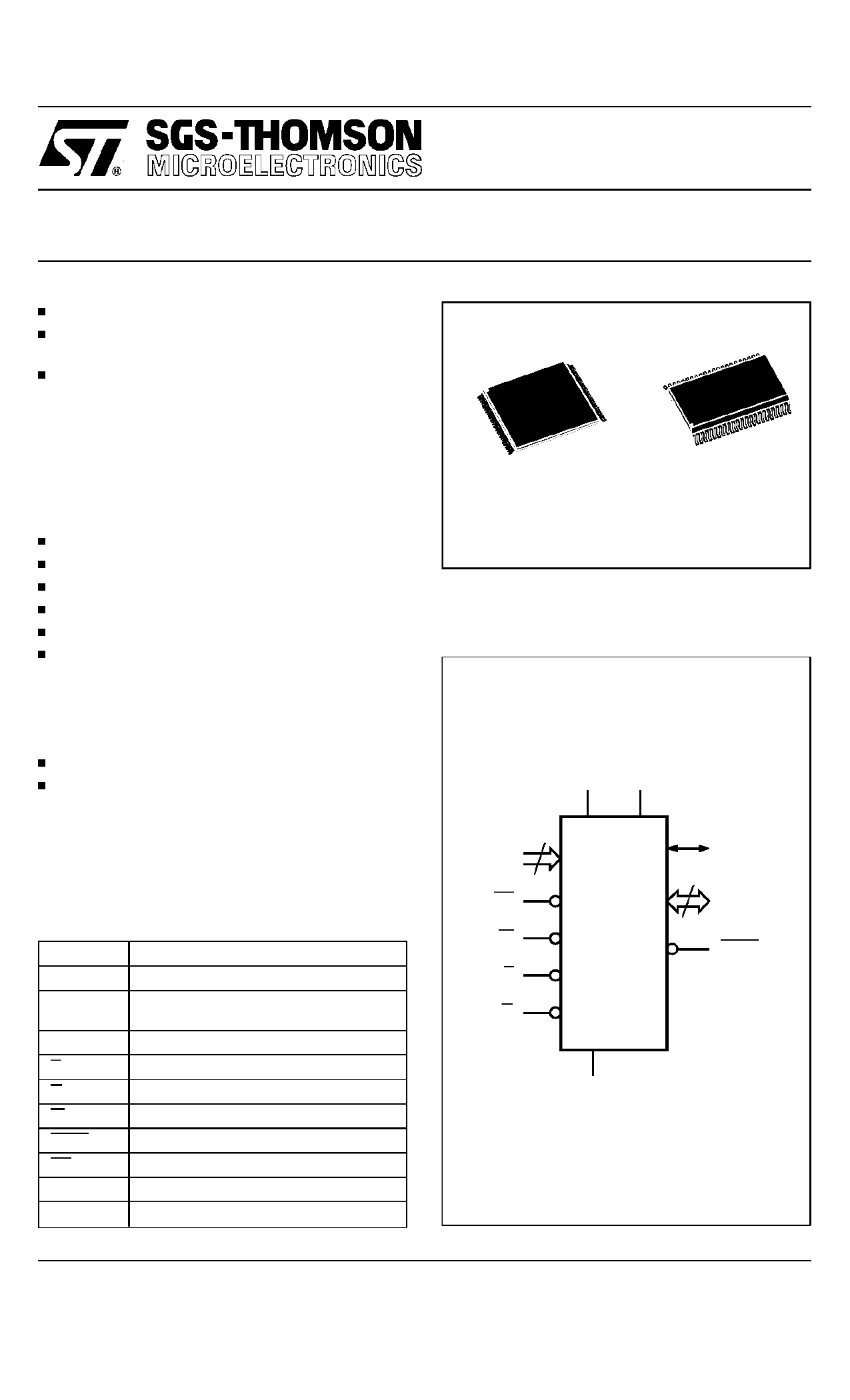
TSOP56 (N)
14 x 20mm
44
1
SO44 (M)
Figure 1. Logic Diagram
VCC VPP
Table 1. Signal Names
A0-A17
DQ0-DQ7
DQ8-
DQ14
DQ15A-1
E
G
W
BYTE
RP
VPP
VCC
Address Inputs
Data Input / Outputs
Data Input / Outputs
Data Input/Output or Address Input
Chip Enable
Output Enable
Write Enable
Byte/Word Organization
Reset/Power Down/Boot Block Unlock
Program & Erase Supply Voltage
Supply Voltage
18
A0-A17
RP
W
E
G
M28F410
M28F420
DQ15A-1
15
DQ0-DQ14
BYTE
VSS
AI01130C
March 1995
This is preliminary infor mationon a new product now in developmen t or undergoing evaluation. Details are subject to change without notice.
1/38
1 page 
M28F410, M28F420
Table 7. Status Register
Mne-
monic
P/ECS
Bit
Name
Logic
Level
Definition
7 P/E.C. Status
’1’ Ready
’0’ Busy
ESS
ES
Erase
6 Suspend
Status
5 Erase Status
’1’ Suspended
’0’
In progress or
Completed
’1’ Erase Error
’0’ Erase Success
PS
4
Program
Status
VPPS
3 VPP Status
’1’ Program Error
’0’
Program
Success
’1’ VPP Low, Abort
’0’ VPP OK
2 Reserved
1 Reserved
0 Reserved
Notes: Logic level ’1’ is High, ’0’ is Low.
Note
Indicates the P/E.C. status, check during Program
or Erase, and on completion before checking bits
b4 or b5 for Program or Erase Success
On an Erase Suspend instruction P/ECS and
ESS bits are set to ’1’. ESS bit remains ’1’ until an
Erase Resume instruction is given.
ES bit is set to ’1’ if P/E.C. has applied the
maximum number of erase pulses to the block
without achieving an erase verify.
PS bit set to ’1’ if the P/E.C. has failed to program
a byte or word.
VPPS bit is set if the VPP voltage is below
VPPH(min) when a Program or Erase instruction
has been executed.
is first applied, on exit from power down or if VCC
falls below VLKO, the command interface is reset to
Read Memory Array.
Instructions and Commands
Eight Instructions are defined to perform Read
Memory Array, Read Status Register, Read Elec-
tronic Signature, Erase, Program, Clear Status
Register, Erase Suspend and Erase Resume. An
internalProgram/EraseController (P/E.C.) handles
all timing and verification of the Program and Erase
instructions and provides status bits to indicate its
operation and exit status. Instructions are com-
posed of a first command write operation followed
by either second command write, to confirm the
commands for programming or erase, or a read
operationto read data from the array, the Electronic
Signature or the Status Register.
For added data protection, the instructions for byte
or word program and block erase consist of two
commands that are written to the memory and
which start the automatic P/E.C. operation. Byte or
word programming takes typically 9μs, block erase
typically 1 second. Erasure of a memory block may
be suspended in order to read data from another
block and then resumed. A Status Register may be
read at any time, including during the programming
or erase cycles, to monitor the progress of the
operation.
Power Saving
The M28F410 and M28F420 have a number of
power saving features. A CMOS standby mode is
entered when the Chip Enable E and the Re-
set/Power Down (RP) signals are at VCC, when the
supply current drops to typically 60μA. A deep
power down mode is enabled when the Re-
set/Power Down (RP) signal is at VSS, when the
supply current drops to typically 0.2μA. The time
required to awake from the deep power down mode
is 300ns maximum, with instructions to the C.I.
recognised after only 210ns.
5/38
5 Page 
M28F410, M28F420
Table 14. Read AC Characteristics (1)
(TA = –40 to 125°C; VPP = 12V ± 5%)
Symbol Alt
Parameter
M28F410 / 20
-80
-90
-100
-120
VCC = 5V ± 5% VCC = 5V ± 10% VCC = 5V ± 10% VCC = 5V ± 10% Unit
SRAM
Interface
EPROM
Interface
EPROM
Interface
EPROM
Interface
Min Max Min Max Min Max Min Max
tAVAV
tRC
Address Valid to
Next Address Valid
80
90 100 120 ns
tAVQV
tACC
Address Valid to
Output Valid
80 90 100 120 ns
tPHQV
tPWH
Power Down High
to Output Valid
300 300 300 300 ns
tELQX (2)
tLZ
Chip Enable Low to
Output Transition
0
0
0
0 ns
tELQV (3)
tCE
Chip Enable Low to
Output Valid
80
90 100 120 ns
tGLQX (2)
tOLZ
Output Enable Low
to Output Transition
0
0
0
0 ns
tGLQV (3)
tOE
Output Enable Low
to Output Valid
40
45
50
55 ns
tEHQX (2)
tOH
Chip Enable High
to Output Transition
0
0
0
0 ns
tEHQZ (2)
tHZ
Chip Enable High
to Output Hi-Z
30 35 40
45 ns
tGHQX (2)
tOH
Output Enable High
to Output Transition
0
0
0
0 ns
tGHQZ (2)
tDF
Output Enable High
to Output Hi-Z
30
35
40
45 ns
tAXQX (2)
tOH
Address Transition
to Output Transition
0
0
0
Notes: 1. See Figure 3 and Table 8 for timing measurements.
2. Sampled only, not 100% tested.
3. G may be delayed by up to tELQV - tGLQV after the falling edge of E without increasing tELQV.
0
ns
11/38
11 Page | ||
| Páginas | Total 30 Páginas | |
| PDF Descargar | [ Datasheet 28F410-100M1.PDF ] | |
Hoja de datos destacado
| Número de pieza | Descripción | Fabricantes |
| 28F410-100M1 | M28F410 | ETC |
| Número de pieza | Descripción | Fabricantes |
| SLA6805M | High Voltage 3 phase Motor Driver IC. |
Sanken |
| SDC1742 | 12- and 14-Bit Hybrid Synchro / Resolver-to-Digital Converters. |
Analog Devices |
|
DataSheet.es es una pagina web que funciona como un repositorio de manuales o hoja de datos de muchos de los productos más populares, |
| DataSheet.es | 2020 | Privacy Policy | Contacto | Buscar |