|
|
|
PDF MC33128 Data sheet ( Hoja de datos )
| Número de pieza | MC33128 | |
| Descripción | POWER MANAGEMENT CONTROLLER | |
| Fabricantes | Motorola Semiconductors | |
| Logotipo | ||
Hay una vista previa y un enlace de descarga de MC33128 (archivo pdf) en la parte inferior de esta página. Total 8 Páginas | ||
|
No Preview Available !
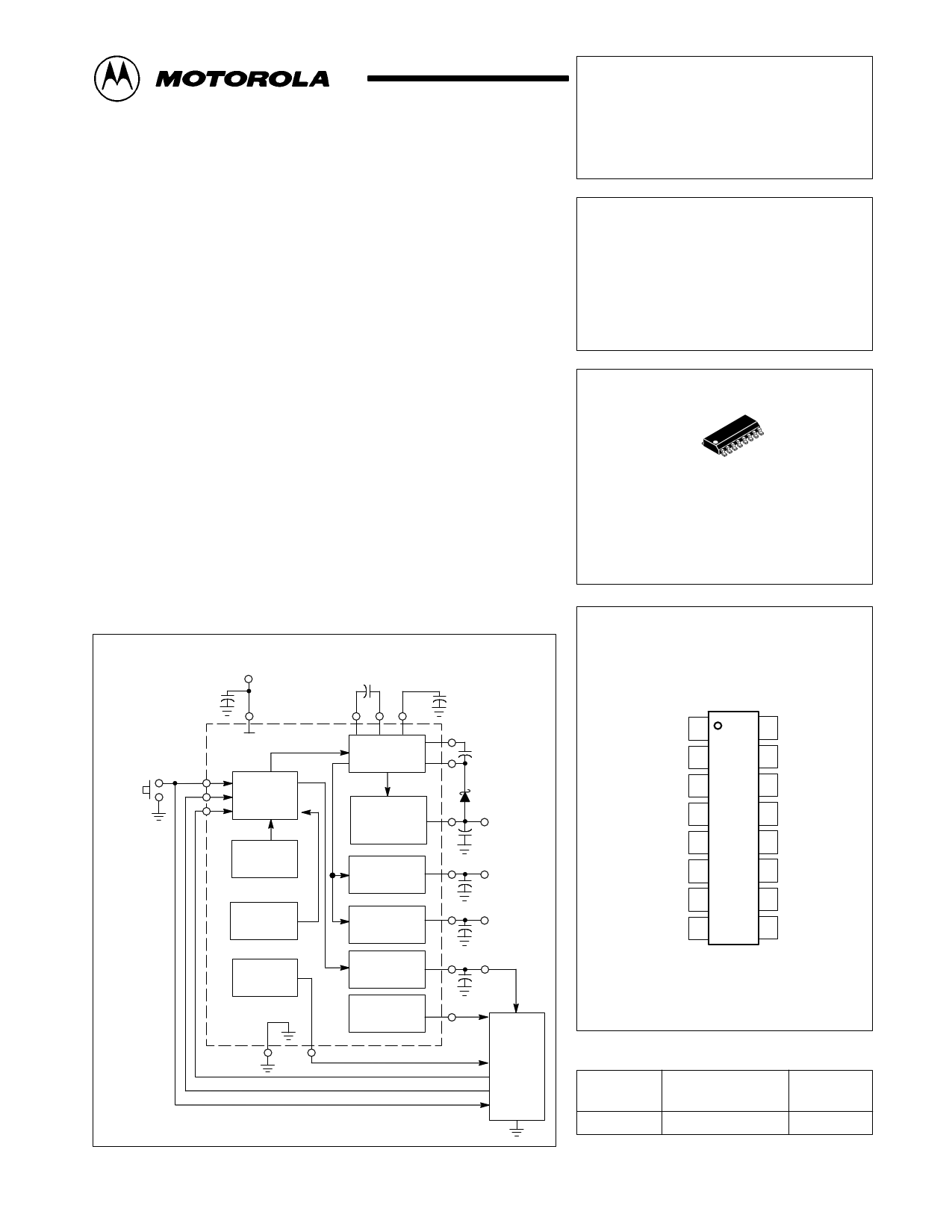
Power Management Controller
The MC33128 is a power management controller specifically designed for
use in battery powered cellular telephone and pager applications. This
device contains all of the active functions required to interface the user to the
system electronics via a microprocessor. This integrated circuit consists of a
low dropout voltage regulator with power–up reset for MPU power, two low
dropout voltage regulators for independant powering of analog and digital
circuitry, and a negative charge pump voltage regulator for full depletion of
gallium arsenide MESFETs.
Also included are protective system shutdown features consisting of a
battery latch that is activated upon battery insertion, low battery voltage
shutdown, and a thermal over temperature detector. This device is available
in a 16–pin narrow body surface mount plastic package.
• Three Positive Regulated Outputs Featuring Low Dropout Voltage
• Negative Regulated Output for Full Depletion of GaAs MESFETs
• MPU Power Up Reset
• Battery Latch
• Low Battery Shutdown
• Pinned–Out Reference for MPU A/D Converter
• Low Start–Up and Operating Current
• Thermal Protection
Order this document by MC33128/D
MC33128
POWER MANAGEMENT
CONTROLLER
SEMICONDUCTOR
TECHNICAL DATA
16
1
D SUFFIX
PLASTIC PACKAGE
CASE 751B
(SO–16)
ON/OFF
Toggle
Simplified Block Diagram
VCC VBB CPC
16
+
11
10 Control
9 Logic
Low Battery
Shutdown
Thermal
Protection
Reference
32
4
Charge
Pump
Negative
Standby
Regulator
Standby
Regulator 1
Standby
Regulator 2
MPU
Regulator
MPU Power
Up Reset
Gnd 6 12 Reference Output
MOTOROLA ANALOG IC DEVICE DATA
PIN CONNECTIONS
VBB Output
8
Output 4
CPC
7
5 Output 4
–2.5 V/1.0 mA
15 Output 1
3.0 V/30 mA
1 Output 2
3.0 V/60 mA
Output 3
14 3.0 V/20 mA
13
R VDD
Output 2 1
VBB Charge Pump
Capacitor Input
2
VBB Charge Pump
Capacitor Drive
3
VBB Output 4
Output 4 5
Gnd 6
Output 4 Charge Pump
Capacitor Input
7
Output 4 Charge Pump 8
Capacitor Drive
16 VCC
15 Output 1
14 Output 3
13 Reset Output
12 Reference Output
11 Power Up Input
10 Power Down Input
9 Battery Saver Input
(Top View)
I MPU
O
O
I VSS
ORDERING INFORMATION
Device
Operating
Temperature Range Package
MC33128D TA = – 30° to +60°C
SO–16
© Motorola, Inc. 1996
Rev 0
1
1 page 
MC33128
OPERATING DESCRIPTION
The MC33128 is a complete power management
controller that is designed to interface the user to the system
electronics via a microprocessor.
Outputs
Three low dropout voltage regulators are provided at outputs
1, 2 and 3. Outputs 1 and 2 were contemplated for independent
powering of the systems analog and digital circuitry. This
significantly reduces the possibility of digitally generated noise
and spurious signals from coupling into the RF and analog
circuits. The low dropout characteristic of Outputs 1 and 2 is
achieved by applying a boosted battery voltage, VBB, to their
respective driver transistors. This allows the output pass
transistors to be driven into saturation when the battery voltage
approaches 3.0 V. The VBB Output appears at Pin 4 and can be
used to provide gate bias for enhancing external N channel
MOSFET switches. Excessive loading of the VBB output will
result in an increase in dropout voltage.
Output 4 is derived from a voltage inverting charge pump
circuit and is intended to provide the negative gate bias
required for full depletion of RF gallium arsenide MESFETs.
In personal communication system applications such as
cellular telephone, negative gate bias is usually required by
the antenna switch and power amplifier circuit blocks with a
typical combined current of less than 1.0 mA. Output 4 can
supply in excess of 2.0 mA, but there will be an increase in
dropout voltage of Outputs 1, 2 and 3.
Outputs 1, 2, 4, VBB Generator and Thermal Protection are
all enabled and disabled in unison by the Battery Saver Input,
Pin 9. The microprocessor can be programmed to
significantly extend the system battery operating time by
periodically enabling the receiver circuitry.
Output 3 provides power to the microprocessor, flash
EPROM and the system display. These blocks are enabled
by the Power Up Input, Pin 11, and disabled by the Power
Down Input, Pin 10. By having separate power up and power
down inputs, the microprocessor can store any pending
information before turning the system and then itself OFF.
This allows a controlled or graceful shutdown. Note that the
power down request is initiated by pressing the toggle switch
while the system is “ON”. This action generates a
microprocessor non–maskable interrupt that initiates the
graceful shutdown.
Battery Voltage Detection
Reverse biasing and eventual failure of the lowest
capacity cell in the battery pack can occur if the system is
accidentally left on for an extended time period. To prevent
this condition the following circuit blocks were incorporated.
A means for low battery detection is accomplished by
using the Reference Output, Pin 12, in conjunction with the
microprocessor’s analog to digital converter input. A
microprocessor output (LBO) can be designated to flash a
display enunciator when a low battery condition exists. The
Reference Output is 1.5 V ± 2.7% and is capable of sourcing
in excess of 10 mA.
The Power Up Reset Output, Pin 13, is designed to hold
the microprocessor reset input low until the voltage at Output 3
rises above 2.66 V. This feature prevents the microprocessor
from hanging or writing invalid information into its memory
during power up. Notice that the output of the MPU Power Up
Reset comparator also drives the base of transistor QPD. If
Output 3 should fall below 2.6 V, due to an overload or a low
battery condition, the comparator will drive QPD “ON”,
causing its collector to pull high on the Power Down Input,
immediately forcing the system into standby mode.
Externally pulling down on Pin 13, base of QPD, will also force
the system into standby mode.
A redundant Low Battery Shutdown circuit is included.
This circuit directly monitors the battery voltage and also
forces the system into standby mode when the battery
voltage falls below 2.4 V. To test the functionality of this
circuit, the high state signal generated by transistor QPD must
be clamped low, to prevent resetting the ON/OFF Latch. An
external short or a pull–down, capable of sinking 2.0 mA at
less than 0.8 V, must be connected to Pin 10.
A Battery Latch circuit is designed into the IC to prevent
the system from turning on when the batteries are inserted
into the finished product. This feature is useful for the end
customer as well as the equipment manufacturer. Upon initial
application of battery voltage, the lower comparator (0.7 V
threshold) forces the Battery Latch into a reset state with its
“Q” output low. This in turn triggers a reset of the ON/OFF
Latch via the OR gate and also locks out the set signal
present at the upper input of the AND gate. As the voltage at
Pin 11 rises above (VCC – 1.5 V), the set signal disappears,
leaving the state of the ON/OFF Latch unchanged (reset).
When the voltage at Pin 11 rises above (VCC – 1.0 V), the
upper comparator forces the Battery Latch into a set state
causing its “Q” output to go high. This allows the AND gate
and the ON/OFF Latch to receive a set signal from Pin 11.
The initial Battery Latch lockout time is controlled by the
internal 20 kΩ resistor and the external 0.1 µF capacitor.
MOTOROLA ANALOG IC DEVICE DATA
5
5 Page | ||
| Páginas | Total 8 Páginas | |
| PDF Descargar | [ Datasheet MC33128.PDF ] | |
Hoja de datos destacado
| Número de pieza | Descripción | Fabricantes |
| MC33121 | LOW VOLTAGE SUBSCRIBER LOOP INTERFACE CIRCUIT | Motorola Semiconductors |
| MC33128 | POWER MANAGEMENT CONTROLLER | Motorola Semiconductors |
| MC33129 | HIGH PERFORMANCE CURRENT MODE CONTROLLERS | Motorola Semiconductors |
| MC33129 | (MC33129 / MC34129) High Performance Current Mode Controller | Motorola Semiconductors |
| Número de pieza | Descripción | Fabricantes |
| SLA6805M | High Voltage 3 phase Motor Driver IC. |
Sanken |
| SDC1742 | 12- and 14-Bit Hybrid Synchro / Resolver-to-Digital Converters. |
Analog Devices |
|
DataSheet.es es una pagina web que funciona como un repositorio de manuales o hoja de datos de muchos de los productos más populares, |
| DataSheet.es | 2020 | Privacy Policy | Contacto | Buscar |