|
|
|
PDF MC33143 Data sheet ( Hoja de datos )
| Número de pieza | MC33143 | |
| Descripción | DUAL HIGH-SIDE SWITCH | |
| Fabricantes | Motorola Semiconductors | |
| Logotipo | ||
Hay una vista previa y un enlace de descarga de MC33143 (archivo pdf) en la parte inferior de esta página. Total 8 Páginas | ||
|
No Preview Available !
Order this document by MC33143/D
Advance Information
Dual High-Side Switch
MC33143
The MC33143 is a dual high–side switch designed for solenoid control in
harsh automotive applications, but is well suited for other environments. The
device can also be used to control small motors and relays as well as
solenoids. The MC33143 incorporates SMARTMOS™ technology, with
CMOS logic, bipolar/MOS analog circuitry, and DMOS power outputs. An
internal charge pump is incorporated for efficient gate enhancement of the
internal high–side power output devices. The outputs are designed to
provide current to low impedance solenoids. The MC33143 provides
individual output fault status reporting along with internal Overcurrent and
Over Temperature protection. The device also has Overvoltage protection,
with automatic recovery, which “globally” disables both outputs for the
duration of an Overvoltage condition. Each output has individual Overcurrent
and Over Temperature shutdown with automatic retry recovery. Outputs are
enabled with a CMOS logic high signal applied to an input to providing true
logic control. The outputs, when turned on, provide full supply (battery)
voltage across the solenoid coil.
The MC33143 is packaged in an economical 24 pin surface mount power
package and specified over an operating voltage of 5.5 V ≤ VPwr < 26 V for
–40°C ≤ TA ≤ 125°C.
• Designed to Operate Over Wide Supply Voltages of 5.5 V to 26 V
• Dual High–Side Outputs Clamped to –10 V for Driving Inductive Loads
• Internal Charge Pump for Enhanced Gate Drive
• Interfaces Directly to a Microcontroller with Parallel Input Control
• Outputs Current Limited to 3.0 A to 6.0 A for Driving Incandescent Loads
• Chip Enable “Sleep Mode” for Power Conservation
• Individual Output Status Reporting
• Fault Interrupt Output for System Interrupt Use
• Output ON or OFF Open Load Detection
• Overvoltage Detection and Shutdown
• Output Over Temperature Detection and Shutdown with Automatic Retry
• Sustained Current Limit or Immediate Overcurrent Shutdown Output Modes
• Output Short to Ground Detection and Shutdown with Automatic Retry
• Output Short to VPwr Detection
SMARTMOS is a trademark of Motorola, Inc.
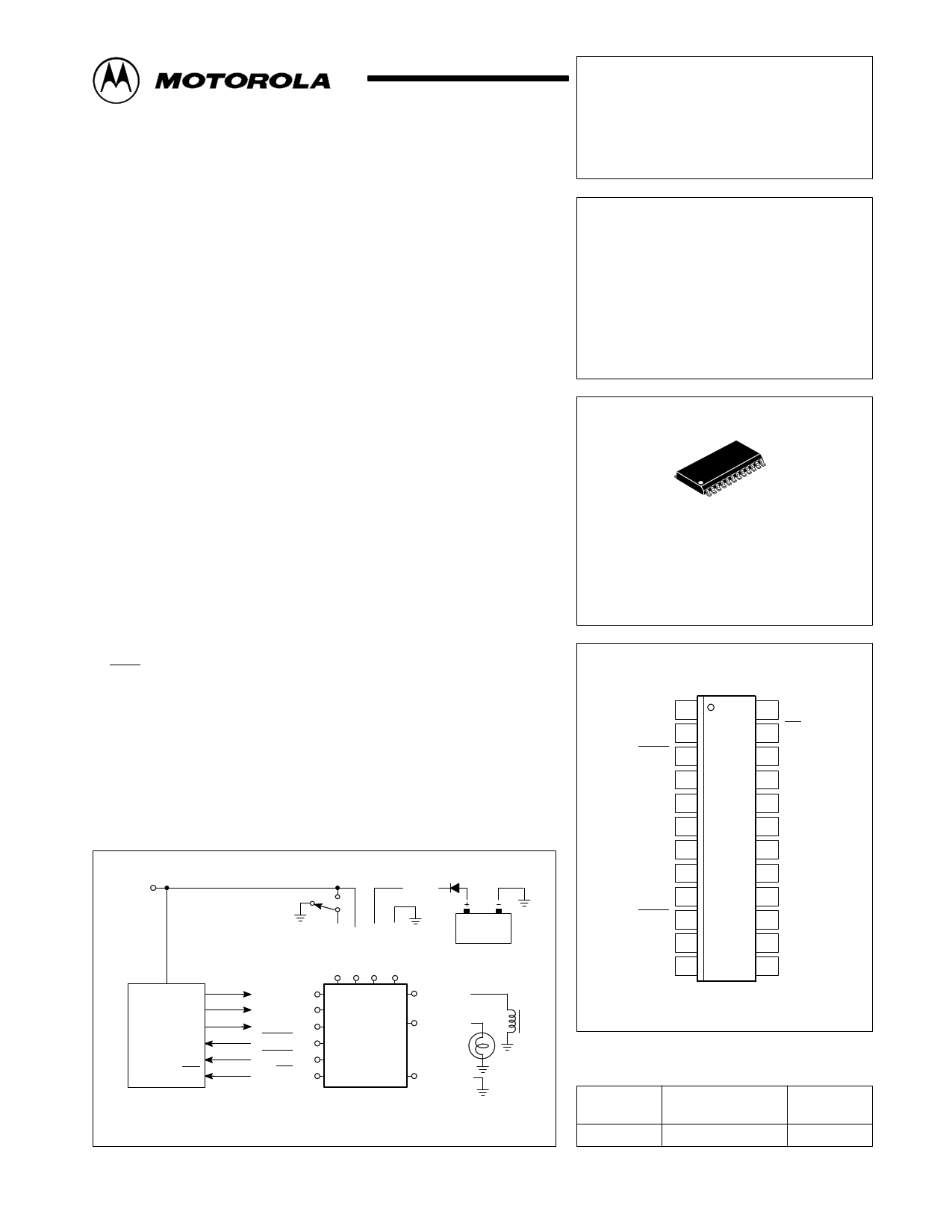
Simplified Application
VDD +VPwr
Battery
DUAL HIGH–SIDE
SWITCH
SEMICONDUCTOR
TECHNICAL DATA
24
1
DW SUFFIX
PLASTIC PACKAGE
CASE 751E
(SOP (16+4+4)L)
PIN CONNECTIONS
IN1 1
CEN 2
STAT1 3
VPwr 4
Gnd 5
Gnd 6
Gnd 7
Gnd 8
VPwr 9
STAT2 10
VDD 11
IN2 12
24 OUT1
23 INT
22 N/C
21 VPwr
20 Gnd
19 Gnd
18 Gnd
17 Gnd
16 VPwr
15 GTST
14 SFPD
13 OUT2
VDD P0
P1
P2
MCU P3
P4
IRQ
CEN (2)
IN1 (1)
IN2 (12)
STAT1 (13)
STAT2 (10)
INT (23)
MC33143
OUT1 (24)
OUT2 (13)
Gnd (Note)
NOTE: Pins 5, 6, 7, 8, 17, 18, 19 and 20 provide electrical ground and heatsinking.
This device contains 889 active transistors.
(Top View)
ORDERING INFORMATION
Device
Operating
Temperature Range Package
MC33143DW TA = – 40° to +125°C SOP–24L
This document contains information on a new product. Specifications and information herein
arMe sOubTjeOctRtoOcLhaAngAe NwiAthLouOt nGotiIcCe. DEVICE DATA
© Motorola, Inc. 1996
Rev 0
1
1 page 
MC33143
Figure 2. Output Response Waveform
5.0 V
IN1–2
50%
0V
tdlh
VPwr
OUT1–2
VPwr – 3.0 V
0 V 2.0 V
tSRr
tdhl
tSRf
PIN FUNCTION DESCRIPTION
Pin
ÁÁÁÁÁÁÁÁÁÁÁÁÁÁÁÁÁÁÁÁÁÁÁÁÁÁÁÁÁÁÁÁÁÁÁÁÁÁÁÁÁÁÁÁÁÁÁÁÁÁÁÁÁÁÁÁÁÁÁÁÁÁÁÁÁÁÁÁÁÁÁÁÁÁÁÁÁÁÁÁÁÁÁÁÁÁÁÁÁÁÁÁÁÁÁÁÁÁÁÁÁÁÁÁÁÁÁÁÁÁÁÁÁÁÁÁÁÁÁÁÁÁÁÁÁÁÁÁÁÁÁÁÁÁÁÁ1, 12
Symbol
IN1, IN2
Description
INput 1 and INput 2 (IN1 and IN2) respectively determine the state of the corresponding output drivers
(OUT1 and OUT2) under normal operating conditions. When an input is high, it’s corresponding output
is active ON, and when low is disabled OFF. IN1 and IN2 have internal active pull–downs which allow a
floating input pin to be conservatively interpreted as a logic low, turning Off the output. An unused input
should be connected to ground.
2 CEN
Chip Enable (CEN) input pin, when low, disables both outputs (OUT1 and OUT2) and places the device
in a “sleep mode” reducing the bias current required from VDD and VPwr. A falling edge of CEN causes
OUT1 and OUT2 to rapidly turn OFF. A falling edge of CEN should precede any VDD shutdown to allow
time OUT1 and OUT2 to be disabled. When CEN is low, INTerrupt (INT) and STATus 1 and 2 (STAT1–2)
will be tri–stated (high impedance). The CEN pin can also be used for power–on reset and under
voltage lockout to disable the outputs for power supply voltages less than 4.5 V. CEN is a dependent
input from the system microcontroller unit (MCU) or some other integrated circuit. It has an internal
pull–up resistor to VDD affording a floating pin to be interpreted as a logic high. Rpull–up is greater than
50 kΩ. If used externally, this pin should be connected to VDD.
3, 10
STAT1. STAT2
The STATus pins (STAT1–2) respectively indicate the presence of faults on OUT1–2. STAT1–2 will be
logic high during normal operation. A logic low will occur whenever an Open Load, Short–to–Ground,
Short–to–Supply (Battery), Thermal Limit, or Overvoltage Shutdown fault condition is experienced on a
corresponding output. STAT1–2 are both active low digital drivers. A 10 kΩ resistor between STAT1–2
and the system CPU may improve a Failure Mode Evaluation Analysis (FMEA) score if STAT1–2 are
externally shorted to VPwr. If unused, this pin should be left connected.
4, 9, 16, VPwr
These pins are connected to the supply and provide load current to the DMOS outputs, are used
21 pumping the DMOS gates, and for Overvoltage shutdown detection of the DMOS. The DMOS outputs
will turn ON with 5.5 to 24 V applied to VPwr. VPwr is limited to –1.5 V for a maximum duration of
5, 6, 7, 8,
ÁÁÁÁÁÁÁÁÁÁÁÁÁÁÁÁÁÁÁÁÁÁÁÁÁÁÁÁÁÁÁÁÁÁ17, 18,
ÁÁÁÁÁÁÁÁÁÁÁÁÁÁÁÁÁÁÁÁÁÁÁÁÁÁÁÁÁÁÁÁÁÁ19, 20
ÁÁÁÁÁÁÁÁÁÁÁÁÁÁÁÁÁÁÁÁÁÁÁÁÁÁÁÁÁÁÁÁÁÁ11
Gnd
VDD
ÁÁÁÁÁÁÁÁÁÁÁÁÁÁÁÁÁÁÁÁÁÁÁÁÁÁÁÁÁÁÁÁÁÁÁÁÁÁÁÁÁÁÁÁÁÁÁÁÁÁÁÁÁÁÁÁÁÁÁÁÁÁÁÁÁÁÁÁÁÁÁÁÁÁÁÁÁÁÁÁÁÁÁÁÁÁÁÁÁÁÁÁÁÁÁÁÁÁÁÁÁÁÁÁÁÁÁÁÁÁÁÁÁÁÁÁÁÁÁÁÁÁÁÁÁÁÁÁÁÁÁÁÁÁÁÁÁÁÁÁÁÁÁÁÁÁÁÁÁÁÁÁÁÁÁÁÁÁÁÁÁÁÁÁÁÁÁÁÁÁÁÁÁÁÁÁÁÁÁÁÁÁÁÁÁÁÁÁÁÁÁÁÁÁÁÁÁÁÁÁÁÁÁÁÁÁÁÁÁÁÁÁÁÁÁÁÁÁÁÁÁÁÁÁÁÁÁÁÁÁÁÁÁÁÁÁÁÁ13,24 OUT1,OUT2
250 ms. A 10 nF de–coupling cap is recommended to be used from VPwr to Ground.
These eight pins constitute the circuits ground (Gnd) and also provide heatsinking for the DMOS output
transistors. Ground continuity is required for the outputs2 to turn ON.
This pin is to be connected to the 5.0 V logic supply of the system. A 10 nF de–coupling capacitor is
recommended from VDD to Gnd.
These pins are connected internally to the DMOS output transistors which source current into the
corresponding load. Each output incorporates dynamic clamping to accommodate inductive loads. In
addition, each output has independent short to ground detection and protection, current limit detection
and protection, thermal limit detection and protection, ON open load and or short to supply (battery)
detection. Neither output will turn ON if CEN is logic low. An unused output should be connected to a
10 kΩ load to prevent false fault reporting. A 1.0 nF filter capacitor may be used from OUT to Gnd to
provide dV/dt noise filtering.
MOTOROLA ANALOG IC DEVICE DATA
5
5 Page | ||
| Páginas | Total 8 Páginas | |
| PDF Descargar | [ Datasheet MC33143.PDF ] | |
Hoja de datos destacado
| Número de pieza | Descripción | Fabricantes |
| MC33143 | DUAL HIGH-SIDE SWITCH | Motorola Semiconductors |
| Número de pieza | Descripción | Fabricantes |
| SLA6805M | High Voltage 3 phase Motor Driver IC. |
Sanken |
| SDC1742 | 12- and 14-Bit Hybrid Synchro / Resolver-to-Digital Converters. |
Analog Devices |
|
DataSheet.es es una pagina web que funciona como un repositorio de manuales o hoja de datos de muchos de los productos más populares, |
| DataSheet.es | 2020 | Privacy Policy | Contacto | Buscar |