|
|
|
PDF ICX434DQN Data sheet ( Hoja de datos )
| Número de pieza | ICX434DQN | |
| Descripción | Diagonal 5.68mm (Type 1/3.2) Frame Readout CCD Image Sensor | |
| Fabricantes | Sony | |
| Logotipo | ||
Hay una vista previa y un enlace de descarga de ICX434DQN (archivo pdf) en la parte inferior de esta página. Total 23 Páginas | ||
|
No Preview Available !
ICX434DQN
Diagonal 5.68mm (Type 1/3.2) Frame Readout CCD Image Sensor with Square Pixel for Color Cameras
Description
The ICX434DQN is a diagonal 5.68mm (Type
1/3.2) interline CCD solid-state image sensor with a
square pixel array and 2.02M effective pixels. Frame
readout allows all pixels' signals to be output
independently within approximately 1/7.5 second.
Also, the adoption of high frame rate readout mode
supports 30 frames per second which is four times
the speed in frame readout mode. This chip features
an electronic shutter with variable charge-storage
time. Adoption of a design specially suited for frame
readout ensures a saturation signal level equivalent
to when using field readout. High resolution and high
color reproductivity are achieved through the use of
R, G, B primary color mosaic filters. Further, high
sensitivity and low dark current are achieved through
the adoption of Super HAD CCD technology.
This chip is suitable for applications such as electronic
still cameras, PC input cameras, etc.
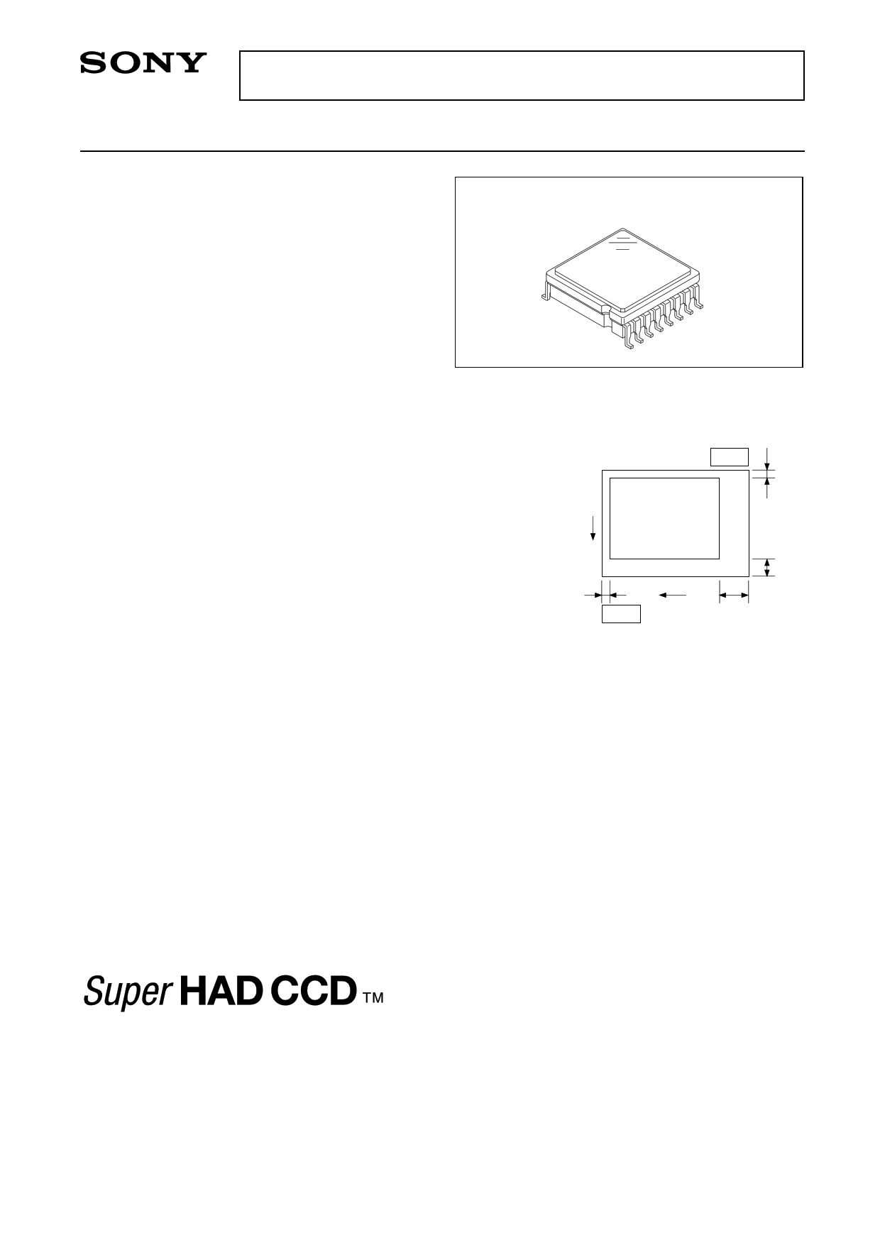
16 pin SOP (Plastic)
Pin 1
2
Features
• Supports frame readout
V
• High horizontal and vertical resolution
• Supports high frame rate readout mode: 30 frames/s
• Square pixel
• Horizontal drive frequency: 18MHz
4
• No voltage adjustments (reset gate and substrate bias are not adjusted.)
Pin 9
H
48
• R, G, B primary color mosaic filters on chip
• High color reproductivity, high sensitivity, low smear
Optical black position
• Continuous variable-speed shutter
(Top View)
• Low dark current, excellent anti-blooming characteristics
• 16-pin high-precision plastic package (top/bottom dual surface reference possible)
10
Device Structure
• Interline CCD image sensor
• Image size:
Diagonal 5.68mm (Type 1/3.2)
• Total number of pixels: 1688 (H) × 1248 (V) approx. 2.11M pixels
• Number of effective pixels: 1636 (H) × 1236 (V) approx. 2.02M pixels
• Number of active pixels: 1620 (H) × 1220 (V) approx. 1.98M pixels
• Chip size:
5.27mm (H) × 4.40mm (V)
• Unit cell size:
2.8µm (H) × 2.8µm (V)
• Optical black:
Horizontal (H) direction: Front 4 pixels, rear 48 pixels
Vertical (V) direction: Front 10 pixels, rear 2 pixels
• Number of dummy bits: Horizontal 28
Vertical 1 (even fields only)
• Substrate material:
Silicon
∗Super HAD CCD is a trademark of Sony Corporation. The Super HAD CCD is a version of Sony's high performance CCD HAD (Hole-
Accumulation Diode) sensor with sharply improved sensitivity by the incorporation of a new semiconductor technology developed by Sony
Corpration.
Sony reserves the right to change products and specifications without prior notice. This information does not convey any license by
any implication or otherwise under any patents or other right. Application circuits shown, if any, are typical examples illustrating the
operation of the devices. Sony cannot assume responsibility for any problems arising out of the use of these circuits.
–1–
E02202
1 page 
ICX434DQN
Drive Clock Waveform Conditions
(1) Readout clock waveform
100%
90%
II II
10%
0%
tr
(2) Vertical transfer clock waveform
VVT
twh
tf
φM
φM
2
Vφ1A, Vφ1B
Vφ3A, Vφ3B
0V
VVH1
VVHH
VVH
VVHL
VVHH
VVHL
VVHL
VVHH
VVHH
VVH3
VVHL
VVH
VVL1
VVLH
VVLL
VVL
Vφ2
VVHH
VVH2 VVHL
VVHH
VVH
VVHL
VVL3
VVL
Vφ4
VVH
VVHH
VVLL
VVLH
VVHH
VVHL
VVHL
VVH4
VVL2VVLH
VVLL
VVL
VVH = (VVH1 + VVH2)/2
VVL = (VVL3 + VVL4)/2
VφV = VVHn – VVLn (n = 1 to 4)
VVLH
VVLL
VVL4
–5–
VVL
5 Page 
ICX434DQN
4. Video signal shading
Set to standard imaging condition III. With the lens diaphragm at F5.6 to F8, adjust the luminous intensity
so that the average value of the Gr signal output is 150mV. Then measure the maximum (Grmax [mV]) and
minimum (Grmin [mV]) values of the Gr signal output and substitute the values into the following formula.
SHg = (Grmax – Grmin)/150 × 100 [%]
5. Dark signal
Measure the average value of the signal output (Vdt [mV]) with the device ambient temperature 60°C and
the device in the light-obstructed state, using the horizontal idle transfer level as a reference.
6. Dark signal shading
After measuring 5, measure the maximum (Vdmax [mV]) and minimum (Vdmin [mV]) values of the dark
signal output and substitute the values into the following formula.
∆Vdt = Vdmax – Vdmin [mV]
7. Line crawl
Set to standard imaging condition II. Adjusting the luminous intensity so that the average value of the Gr
signal output is 150mV, and then insert R, G and B filters and measure the difference between G signal
lines (∆Glr, ∆Glg, ∆Glb [mV]) as well as the average value of the G signal output (Gar, Gag, Gab).
Substitute the values into the following formula.
Lci = ∆Gli/Gai × 100 [%] (i = r, g, b)
8. Lag
Adjust the Gr signal output value generated by strobe light to 150mV. After setting the strobe light so that it
strobes with the following timing, measure the residual signal (Vlag). Substitute the value into the following
formula.
Lag = (Vlag/150) × 100 [%]
VD
Strobe light
timing
Output
Light
Gr signal output 150mV Vlag (lag)
– 11 –
11 Page | ||
| Páginas | Total 23 Páginas | |
| PDF Descargar | [ Datasheet ICX434DQN.PDF ] | |
Hoja de datos destacado
| Número de pieza | Descripción | Fabricantes |
| ICX434DQN | Diagonal 5.68mm (Type 1/3.2) Frame Readout CCD Image Sensor | Sony |
| Número de pieza | Descripción | Fabricantes |
| SLA6805M | High Voltage 3 phase Motor Driver IC. |
Sanken |
| SDC1742 | 12- and 14-Bit Hybrid Synchro / Resolver-to-Digital Converters. |
Analog Devices |
|
DataSheet.es es una pagina web que funciona como un repositorio de manuales o hoja de datos de muchos de los productos más populares, |
| DataSheet.es | 2020 | Privacy Policy | Contacto | Buscar |