|
|
|
PDF CA3078 Data sheet ( Hoja de datos )
| Número de pieza | CA3078 | |
| Descripción | 2MHz / Micropower Operational Amplifier | |
| Fabricantes | Intersil | |
| Logotipo | ||
Hay una vista previa y un enlace de descarga de CA3078 (archivo pdf) en la parte inferior de esta página. Total 12 Páginas | ||
|
No Preview Available !
Data Sheet
CA3078, CA3078A
December 1998
File Number 535.5
2MHz, Micropower Operational Amplifier
The CA3078 and CA3078A are high gain monolithic
operational amplifiers which can deliver milliamperes of
current yet only consume microwatts of standby power. Their
operating points are externally adjustable and frequency
compensation may be accomplished with one external
capacitor. The CA3078 and CA3078A provide the designer
with the opportunity to tailor the frequency response and
improve the slew rate without sacrificing power. Operation
with a single 1.5V battery is a practical reality with these
devices.
The CA3078A is a premium device having a supply voltage
range of V± = 0.75V to V± = 15V. The CA3078 has the same
lower supply voltage limit but the upper limit is V+ = +6V and
V- = -6V.
Ordering Information
PART NUMBER TEMP.
(BRAND)
RANGE (oC)
PACKAGE
CA3078AE
-55 to 125 8 Ld PDIP
CA3078AM
(3078A)
-55 to 125 8 Ld SOIC
PKG.
NO.
E8.3
M8.15
CA3078AM96
(3078A)
CA3078AT
CA3078E
CA3078M
(3078)
CA3078T
-55 to 125 8 Ld SOIC Tape and Reel M8.15
-55 to 125 8 Pin Metal Can
0 to 70 8 Ld PDIP
0 to 70 8 Ld SOIC
T8.C
E8.3
M8.15
0 to 70 8 Pin Metal Can
T8.C
Features
• Low Standby Power . . . . . . . . . . . . . . . As Low As 700nW
• Wide Supply Voltage Range. . . . . . . . . . . ±0.75V to ±15V
• High Peak Output Current . . . . . . . . . . . . . . . 6.5mA (Min)
• Adjustable Quiescent Current
• Output Short Circuit Protection
Applications
• Portable Electronics
• Telemetry
• Medical Electronics
• Intrusion Alarms
• Instrumentation
Pinouts
CA3078 (PDIP, SOIC)
TOP VIEW
COMP 1
INV. INPUT 2
NON-INV.
INPUT
3
V- 4
-
+
8 COMP
7 V+
6 OUTPUT
5 BIAS
CA3078 (METAL CAN)
TOP VIEW
COMP
1
8
TAB
7 V+
V+
RSET
INV.
INPUT
2
+
6 OUTPUT
NON-INV. 3
INPUT
4
V-
NOTE: Case Voltage = Floating
5
BIAS
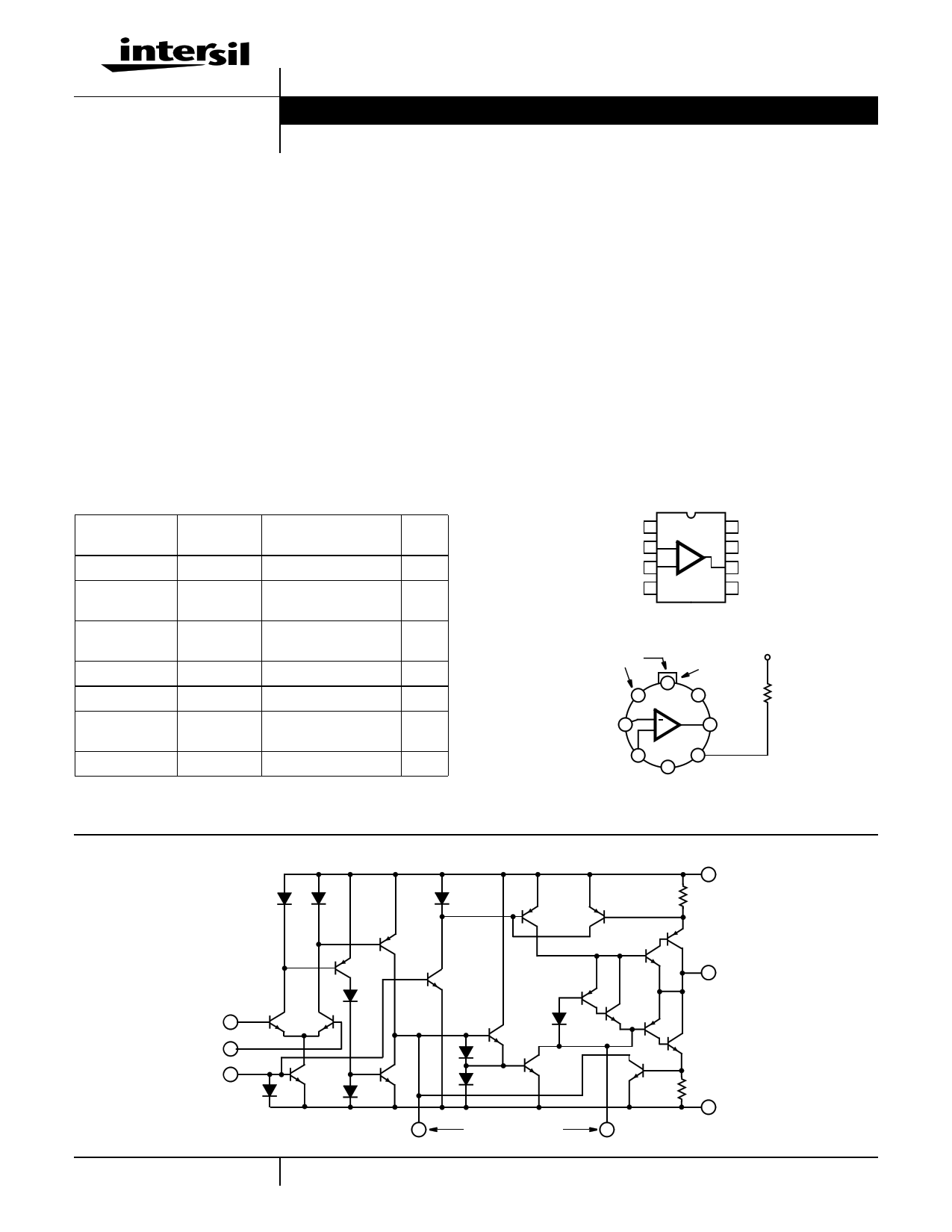
Schematic Diagram
D2
D3
Q4
NON-
INVERTING
3 Q1 Q3
INVERTING
2
BIAS
5
Q2
D1 D4
D9
Q6
Q5
1
D5
Q10 Q12
Q7
Q8
D6
D7
D8
Q9
Q11
Q13
Q14
COMPENSATION
8
7
50Ω V+
Q18
Q16 OUTPUT
6
Q15
Q17
50Ω V-
4
1 CAUTION: These devices are sensitive to electrostatic discharge; follow proper IC Handling Procedures.
1-888-INTERSIL or 321-724-7143 | Copyright © Intersil Corporation 1999
1 page 
CA3078, CA3078A
TABLE 1. UNITY GAIN SLEW RATE vs COMPENSATION - CA3078 AND CA3078A
VSUPPLY = ±6V, Output Voltage (VO) = ±5V, Load Resistance (RL) = 10kΩ, Transient Response: 10% overshoot for an output voltage of 100mV,
Ambient Temperature (TA) = 25oC
UNITY GAIN (INVERTING)
FIGURE 1
UNITY GAIN (NON-INVERTING)
FIGURE 2
COMPENSATION
TECHNIQUE
R1 C1 R2 C2 SLEW RATE R1 C1 R2 C2 SLEW RATE
kΩ pF kΩ µF
V/µs
kΩ pF kΩ µF
V/µs
CA3078 - IQ = 100µA
Single Capacitor
0 750 ∞ 0 0.0085 0 1500 ∞ 0 0.0095
Resistor and Capacitor
3.5 350
∞
0
0.04
5.3 500
∞
0
0.024
Input
∞ 0 0.25 0.306 0.67
∞ 0 0.311 0.45 0.67
CA3078A - IQ = 20µA
Single Capacitor
0 300 ∞ 0 0.0095 0 800 ∞ 0
0.003
Resistor and Capacitor
14 100 ∞
0
0.027
34 125 ∞
0
0.02
Input
∞
0 0.644 0.156
0.29
∞ 0 0.77 0.4
0.4
Application Information
Compensation Techniques
The CA3078A and CA3078 can be phase compensated with
one or two external components depending upon the closed
loop gain, power consumption, and speed desired. The
recommended compensation is a resistor in series with a
capacitor connected from Terminal 1 to Terminal 8. Values of
the resistor and capacitor required for compensation as a
function of closed loop gain are shown in Figures 25 and 26.
These curves represent the compensation necessary at
quiescent currents of 100µA and 20µA, respectively, for a
transient response with 10% overshoot. Figures 23 and 24
show the slew rates that can be obtained with the two different
compensation techniques. Higher speeds can be achieved
with input compensation, but this increases noise output.
Compensation can also be accomplished with a single
capacitor connected from Terminal 1 to Terminal 8, with speed
being sacrificed for simplicity. Table 1 gives an indication of
slew rates that can be obtained with various compensation
techniques at quiescent currents of 100µA and 20µA.
Single Supply Operation
The CA3078A and CA3078 can operate from a single supply
with a minimum total supply voltage of 1.5V. Figures 4 and 5
show the CA3078A or CA3078 in inverting and non-inverting
20dB amplifier configurations utilizing a 1.5V type “AA” cell
for a supply. The total consumption for either circuit is
approximately 675nW. The output voltage swing in this
configuration is 300mVP-P with a 20kΩ load.
Typical Performance Curves
VS = ±6
TA = 25oC
RS ≤ 10kΩ
VS = ±6
10 TA = 25oC
3.0
2.4
1.8
1.2
0.6
0
1
CA3078
CA3078A
10 100
TOTAL QUIESCENT CURRENT (µA)
1000
FIGURE 6. INPUT OFFSET VOLTAGE vs TOTAL QUIESCENT
CURRENT
CA3078
1
0.1
CA3078A
0.01
1
10 100 1000
TOTAL QUIESCENT CURRENT (µA)
10000
FIGURE 7. INPUT OFFSET CURRENT vs TOTAL QUIESCENT
CURRENT
5
5 Page 
CA3078, CA3078A
Small Outline Plastic Packages (SOIC)
N
INDEX
AREA
E
-B-
H
0.25(0.010) M B M
123
-A-
D
SEATING PLANE
A
L
h x 45o
-C-
α
e A1
B 0.10(0.004)
C
0.25(0.010) M C A M B S
NOTES:
11. Symbols are defined in the “MO Series Symbol List” in Section 2.2 of
Publication Number 95.
12. Dimensioning and tolerancing per ANSI Y14.5M-1982.
13. Dimension “D” does not include mold flash, protrusions or gate burrs.
Mold flash, protrusion and gate burrs shall not exceed 0.15mm (0.006
inch) per side.
14. Dimension “E” does not include interlead flash or protrusions. Inter-
lead flash and protrusions shall not exceed 0.25mm (0.010 inch) per
side.
15. The chamfer on the body is optional. If it is not present, a visual index
feature must be located within the crosshatched area.
16. “L” is the length of terminal for soldering to a substrate.
17. “N” is the number of terminal positions.
18. Terminal numbers are shown for reference only.
19. The lead width “B”, as measured 0.36mm (0.014 inch) or greater
above the seating plane, shall not exceed a maximum value of
0.61mm (0.024 inch).
20. Controlling dimension: MILLIMETER. Converted inch dimensions
are not necessarily exact.
M8.15 (JEDEC MS-012-AA ISSUE C)
8 LEAD NARROW BODY SMALL OUTLINE PLASTIC
PACKAGE
INCHES
MILLIMETERS
SYMBOL MIN MAX MIN MAX NOTES
A
0.0532 0.0688 1.35
1.75
-
A1
0.0040 0.0098 0.10
0.25
-
B
0.013 0.020 0.33
0.51
9
C
0.0075 0.0098 0.19
0.25
-
D
0.1890 0.1968 4.80
5.00
3
E
0.1497 0.1574 3.80
4.00
4
e 0.050 BSC 1.27 BSC -
H
0.2284 0.2440 5.80
6.20
-
h
0.0099 0.0196 0.25
0.50
5
L
0.016 0.050 0.40
1.27
6
N8
87
α 0o 8o 0o 8o -
Rev. 0 12/93
11
11 Page | ||
| Páginas | Total 12 Páginas | |
| PDF Descargar | [ Datasheet CA3078.PDF ] | |
Hoja de datos destacado
| Número de pieza | Descripción | Fabricantes |
| CA3070 | (CA3070 - CA3072) Television Chroma System | ETC |
| CA3071 | (CA3070 - CA3072) Television Chroma System | ETC |
| CA3072 | (CA3070 - CA3072) Television Chroma System | ETC |
| CA3075 | FM IF Amplifier-Limiter | Intersil Corporation |
| Número de pieza | Descripción | Fabricantes |
| SLA6805M | High Voltage 3 phase Motor Driver IC. |
Sanken |
| SDC1742 | 12- and 14-Bit Hybrid Synchro / Resolver-to-Digital Converters. |
Analog Devices |
|
DataSheet.es es una pagina web que funciona como un repositorio de manuales o hoja de datos de muchos de los productos más populares, |
| DataSheet.es | 2020 | Privacy Policy | Contacto | Buscar |