|
|
|
PDF CA3059 Data sheet ( Hoja de datos )
| Número de pieza | CA3059 | |
| Descripción | ZERO VOLTAGE SWITCH | |
| Fabricantes | Motorola Semiconductors | |
| Logotipo | ||
Hay una vista previa y un enlace de descarga de CA3059 (archivo pdf) en la parte inferior de esta página. Total 6 Páginas | ||
|
No Preview Available !
Zero Voltage Switch
This series is designed for thyristor control in a variety of AC power
switching applications for AC input voltages of 24 V, 120 V, 208/230 V, and
277 V @ 50/60 Hz.
Applications:
• Relay Control
• Heater Control
• Valve Control
• Lamp Control
• On–Off Motor Switching
• Differential Comparator with Self–Contained Power Supply for Industrial
Applications
• Synchronous Switching of Flashing Lights
Order this document by CA3059/D
CA3059
ZERO VOLTAGE
SWITCH
SEMICONDUCTOR
TECHNICAL DATA
14
1
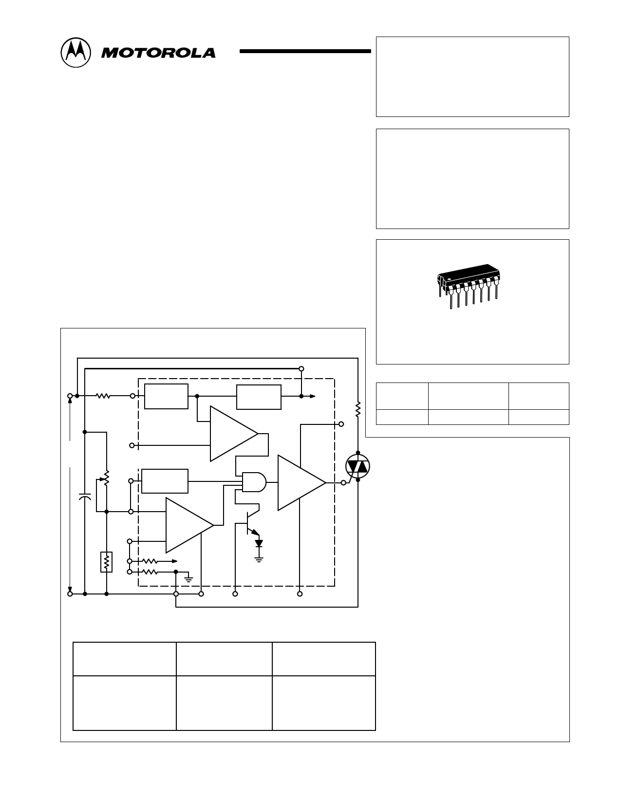
Figure 1. Representative Block Diagram
PLASTIC PACKAGE
CASE 646
RS 5
AC
Input
Limiter
AC
Input
Voltage
100
µF +
15 –
V
*
RX
12
DC Mode or
400 Hz Input
RP 14
Protection
Circuit
13 +
On/Off
Sensing
Amp
9–
10 VCC
11
Power
Supply
Zero
Crossing
Detector
* NTC Sensor
Gnd 7
81
Inhibit
AC Input Voltage
(50/60 Hz)
Vac
24
120
208/230
277
Input Series
Resistor (RS)
kΩ
2.0
10
20
25
2
VCC
VCC
Current
Boost
RL
3
ORDERING INFORMATION
Device
Operating
Temperature Range
Package
CA3059
TA = – 40° to +85°C Plastic DIP
MT2
Triac 4
Drive MT1
Gate
6
External Trigger
Dissipation Rating
for RS
W
0.5
2.0
4.0
5.0
FUNCTIONAL BLOCK
DESCRIPTION
1. Limiter–Power Supply — Allows operation of
the CA3059 directly from an AC line. Suggested
dropping resistor (RS) values are given in the table
below.
2. Differential On/Off Sensing Amplifier — Tests
for condition of external sensors or input command
signals. Proportional control capability or hysteresis
may be implemented using this block.
3. Zero–Crossing Detector — Synchronizes the
output pulses to the zero voltage point of the AC cycle.
This synchronization eliminates RFI when used with
resistive loads.
4. Triac Drive — Supplies high–current pulses to
the external power controlling thyristor.
5. Protection Circuit — A built–in circuit may be
actuated, if the sensor opens or shorts, to remove the
drive current from the external triac.
6. Inhibit Capability — Thyristor firing may be
inhibited by the action of an internal diode gate at
Pin 1.
7. High Power DC Comparator Operation —
Operation in this mode is accomplished by connecting
Pin 7 to Pin 12 (thus overriding the action of the
zero–crossing detector). When Pin 13 is positive with
respect to Pin 9, current to the thyristor is continuous.
MOTOROLA ANALOG IC DEVICE DATA
© Motorola, Inc. 1996
Rev 0
1
1 page 
CF
100 µF
15 V
+
–
2
AC Line
Input
RS
5
85 k
CA3059
Figure 14. Circuit Schematic
RP
Inhibit
Input
1
Rx
NTC Sensor
13
10 k
10
50 k
70 µA
9
9.6 k
11
8
35 µA
15
3 Current
Boost
25
30 k
30 k
30 k
53 µA
150 µA
5k
50 k 4
To
Thyristor
Gate
12
For DC Mode
or 400 Hz
Operation
14
Fail–Safe
Input
7
To
Common
NOTE: Current sources are established by an internal reference.
6
For
External
Trigger
APPLICATION INFORMATION
Power Supply
The CA3059 is a self–powered circuit, powered from the
AC line through an appropriate dropping resistor (see Table
A). The internal supply is designed to power the auxiliary
power circuits.
In applications where more output current from the internal
supply is required, an external power supply of higher voltage
should be used. To use an external power supply, connect
Pin 5 and Pin 7 together and apply the synchronizing voltage
to Pin 12 and the DC supply voltage to Pin 2 as shown in
Figure 4.
Operation of Protection Circuit
The protection circuit, when connected, will remove
current drive from the triac if an open or shorted sensor is
detected. This circuit is activated by connecting Pin 13 to
Pin 14 (see Figure 1).
The following conditions should be observed when the
protection circuit is utilized:
a. The internal supply should be used and the external
load current must be limited to 2 mA with a 5 kΩ
dropping resistor.
b. Sensor Resistance (RX) and RP values should be
between 2 kΩ and 100 kΩ.
c. The relationship 0.33 < RX/RP < 3 must be met over
the anticipated temperature range to prevent
undesired activation of the circuit. A shunt or series
resistor may have to be added.
External Inhibit Function
A priority inhibit command applied to Pin 1 will remove
current drive from the thyristor. A command of at least +1.2 V
@ 10 µA is required. A DTL or TTL logic 1 applied to Pin 1 will
activate the inhibit function.
DC Gate Current Mode
When comparator operation is desired or inductive loads
are being switched, Pins 7 and 12 should be connected. This
connection disables the zero–crossing detector to permit the
flow of gate current from the differential sensing amplifier on
demand. Care should be exercised to avoid possible
overloading of the internal power supply when operating the
device in this mode. A resistor should be inserted between
Pin 4 and the thyristor gate in order to limit the current.
MOTOROLA ANALOG IC DEVICE DATA
5
5 Page | ||
| Páginas | Total 6 Páginas | |
| PDF Descargar | [ Datasheet CA3059.PDF ] | |
Hoja de datos destacado
| Número de pieza | Descripción | Fabricantes |
| CA3050 | (CA3050 / CA3051) Dual Differential Amplifiers | RCA Solid State |
| CA3051 | (CA3050 / CA3051) Dual Differential Amplifiers | RCA Solid State |
| CA3052 | Four Independent AC Amplifiers | ETC |
| CA3053 | (CA3028 / CA3053) Differential/Cascode Amplifiers | Harris Corporation |
| Número de pieza | Descripción | Fabricantes |
| SLA6805M | High Voltage 3 phase Motor Driver IC. |
Sanken |
| SDC1742 | 12- and 14-Bit Hybrid Synchro / Resolver-to-Digital Converters. |
Analog Devices |
|
DataSheet.es es una pagina web que funciona como un repositorio de manuales o hoja de datos de muchos de los productos más populares, |
| DataSheet.es | 2020 | Privacy Policy | Contacto | Buscar |