|
|
PDF DG408 Data sheet ( Hoja de datos )
| Número de pieza | DG408 | |
| Descripción | Single 8-Channel/Differential 4-Channel / CMOS Analog Multiplexers | |
| Fabricantes | Intersil Corporation | |
| Logotipo |  |
|
Hay una vista previa y un enlace de descarga de DG408 (archivo pdf) en la parte inferior de esta página. Total 17 Páginas | ||
|
No Preview Available !
®
Data Sheet
DG408, DG409
June 13, 2006
FN3283.8
Single 8-Channel/Differential 4-Channel,
CMOS Analog Multiplexers
The DG408 Single 8-Channel, and DG409 Differential
4-Channel monolithic CMOS analog multiplexers are drop-in
replacements for the popular DG508A and DG509A series
devices. They each include an array of eight analog
switches, a TTL/CMOS compatible digital decode circuit for
channel selection, a voltage reference for logic thresholds
and an ENABLE input for device selection when several
multiplexers are present.
The DG408 and DG409 feature lower signal ON resistance
(<100Ω) and faster switch transition time (tTRANS < 250ns)
compared to the DG508A or DG509A. Charge injection has
been reduced, simplifying sample and hold applications. The
improvements in the DG408 series are made possible by
using a high-voltage silicon-gate process. An epitaxial layer
prevents the latch-up associated with older CMOS
technologies. Power supplies may be single-ended from +5V
to +34V, or split from ±5V to ±20V.
The analog switches are bilateral, equally matched for AC or
bidirectional signals. The ON resistance variation with
analog signals is quite low over a ±5V analog input range.
Features
• ON Resistance (Max, 25°C). . . . . . . . . . . . . . . . . . . 100Ω
• Low Power Consumption (PD) . . . . . . . . . . . . . . . <11mW
• Fast Switching Action
- tTRANS . . . . . . . . . . . . . . . . . . . . . . . . . . . . . . . . <250ns
- tON/OFF(EN) . . . . . . . . . . . . . . . . . . . . . . . . . . . . <150ns
• Low Charge Injection
• Upgrade from DG508A/DG509A
• TTL, CMOS Compatible
• Single or Split Supply Operation
• Pb-Free Plus Anneal Available (RoHS Compliant)
Applications
• Data Acquisition Systems
• Audio Switching Systems
• Automatic Testers
• Hi-Rel Systems
• Sample and Hold Circuits
• Communication Systems
• Analog Selector Switch
Ordering Information
PART
NUMBER
PART
MARKING
TEMP.
RANGE (°C)
PACKAGE
PKG.
DWG. #
DG408DJ
DG408DJ
-40 to 85
16 Ld PDIP
E16.3
DG408DJZ (Note)
DG408DJZ
-40 to 85
16 Ld PDIP** (Pb-free)
E16.3
DG408DY*
DG408DY
-40 to 85
16 Ld SOIC
M16.15
DG408DYZ* (Note)
DG408DYZ
-40 to 85
16 Ld SOIC (Pb-free)
M16.15
DG408DVZ* (Note)
DG408DVZ
-40 to 85
16 Ld TSSOP (Pb-free)
M16.173
DG409DJ
DG409DJ
-40 to 85
16 Ld PDIP
E16.3
DG409DJZ (Note)
DG409DJZ
-40 to 85
16 Ld PDIP** (Pb-free)
E16.3
DG409DY*
DG409DY
-40 to 85
16 Ld SOIC
M16.15
DG409DYZ* (Note)
DG409DYZ
-40 to 85
16 Ld SOIC (Pb-free)
M16.15
DG409DVZ* (Note)
DG409DVZ
-40 to 85
16 Ld TSSOP (Pb-free)
M16.173
*Add “-T” suffix for tape and reel.
**Pb-free PDIPs can be used for through hole wave solder processing only. They are not intended for use in Reflow solder processing applications.
NOTE: Intersil Pb-free plus anneal products employ special Pb-free material sets; molding compounds/die attach materials and 100% matte tin plate
termination finish, which are RoHS compliant and compatible with both SnPb and Pb-free soldering operations. Intersil Pb-free products are MSL
classified at Pb-free peak reflow temperatures that meet or exceed the Pb-free requirements of IPC/JEDEC J STD-020.
1 CAUTION: These devices are sensitive to electrostatic discharge; follow proper IC Handling Procedures.
1-888-INTERSIL or 1-888-468-3774 | Intersil (and design) is a registered trademark of Intersil Americas Inc.
Copyright Intersil Americas Inc. 1993, 1994, 1997, 1999, 2004, 2006. All Rights Reserved
All other trademarks mentioned are the property of their respective owners.
1 page 
DG408, DG409
Electrical Specifications Test Conditions: V+ = +15V, V- = -15V, VAL = 0.8V, VAH = 2.4V, Unless Otherwise Specified (Continued)
PARAMETER
TEST CONDITIONS
TEMP (°C)
(NOTE 5)
MIN
(NOTE 6)
TYP
(NOTE 5)
MAX
UNITS
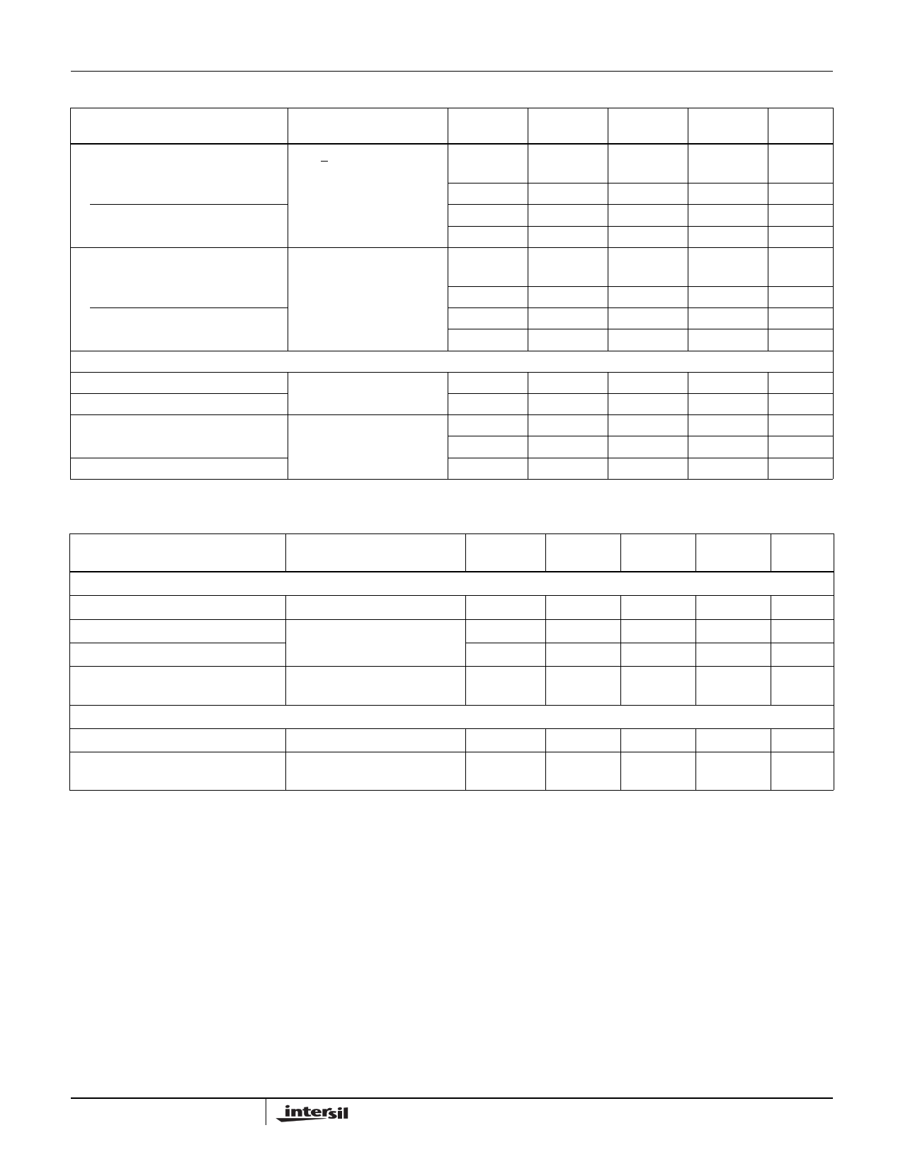
Drain OFF Leakage Current, ID(OFF) VEN = 0V, VD = ±10V,
DG408
VS = +10V
25 -1 - 1 nA
Full -20
-
20 nA
DG409
25 -1 - 1 nA
Full -10
-
10 nA
Drain ON Leakage Current, ID(ON)
VS = VD = ±10V (Note 7)
DG408
25 -1 - 1 nA
Full -20
-
20 nA
DG409
25 -1 - 1 nA
Full -10
-
10 nA
POWER SUPPLY CHARACTERISTICS
Positive Supply Current, I+
Negative Supply Current, I-
VEN = 0V, VA = 0V (Standby)
Full
-
10 75 µA
Full -75
1
- µA
Positive Supply Current, I+
VEN = 2.4V, VA = 0V
(Enabled)
25 - 0.2 0.5 mA
Full - - 2 mA
Negative Supply Current, I-
Full -500
-
- µA
Electrical Specifications Single Supply Test Conditions: V+ = 12V, V- = 0V, VAL = 0.8V, VAH = 2.4V,
Unless Otherwise Specified
PARAMETER
TEST
CONDITION
TEMP (°C)
(NOTE 5)
MIN
(NOTE 6)
TYP
(NOTE 5)
MAX
UNITS
DYNAMIC CHARACTERISTICS
Switching Time of Multiplexer, tTRANS VS1 = 8V, VS8 = 0V, VIN = 2.4V
Enable Turn-ON Time, tON(EN)
Enable Turn-OFF Time, tOFF(EN)
VINH = 2.4V, VINL = 0V,
VS1 = 5V
Charge Injection, Q
CL = 10nF, VGEN = 0V,
RGEN = 0Ω
ANALOG SWITCH CHARACTERISTICS
25
25
25
25
- 180 - ns
- 180 - ns
- 120 - ns
- 5 - pC
Analog Signal Range, VANALOG
Full 0
- 12 V
Drain-Source ON-Resistance,
rDS(ON)
VD = 3V, 10V, IS = -1mA
(Note 7)
25 - 90 - Ω
NOTES:
5. The algebraic convention whereby the most negative value is a minimum and the most positive a maximum, is used in this data sheet.
6. Typical values are for DESIGN AID ONLY, not guaranteed nor production tested.
7. Sequence each switch ON.
8. ∆rDS(ON) = rDS(ON) (Max) - rDS(ON) (Min).
9. Worst case isolation occurs on channel 4 due to proximity to the drain pin.
5 FN3283.8
June 13, 2006
5 Page 
DG408, DG409
Typical Performance Curves (Continued)
20 V+ = 15V
V- = -15V
VIN = 0V
15 VEN = 0V
10
5
0
-55
5 45 85 125
TEMPERATURE (°C)
FIGURE 22. POSITIVE SUPPLY CURRENT vs TEMPERATURE
(DG408)
90
80 CL = 10,000pF
VIN = 5VP-P
70
60
50
40
30
20
10
0
-10
-15
-10
-5
V+ = 15V
V- = -15V
0
VS (V)
V+ = 12V
V- = 0V
5 10
15
FIGURE 23. CHARGE INJECTION vs ANALOG VOLTAGE
120
100
±5V
80
±8V
60 ±10V
±12V
40
20 ±15V
±20V
0
-20 -16 -12
-8
-4 0 4
VD (V)
8 12 16
FIGURE 24. rDS(ON) vs VD AND SUPPLY
20
160
140
V+ = 7.5V
120
100 10V
80 12V
15V
60 20V
40
V- = 0V
20
22V
0
0
4
8 12 16 20 22
VD (V)
FIGURE 25. rDS(ON) vs VD (SINGLE SUPPLY)
80
70
V+ = 15V
V- = -15V
60
125°C
50
85°C
40
25°C
30
20
10
0
-15
0°C
-40°C
-55°C
0
VS (V)
FIGURE 26. rDS(ON) vs VS AND TEMPERATURE
15
130
125°C
110
85°C
90
25°C
70
50
30
10
0
0°C
-40°C
-55°C
V+ = 12V
V- = 0V
48
VS (V)
12
FIGURE 27. rDS(ON) vs VS AND TEMPERATURE
(SINGLE SUPPLY)
11 FN3283.8
June 13, 2006
11 Page | ||
| Páginas | Total 17 Páginas | |
| PDF Descargar | [ Datasheet DG408.PDF ] | |
Hoja de datos destacado
| Número de pieza | Descripción | Fabricantes |
| DG4000 | Function/Arbitrary Waveform Generator Guide Manual | RIGOL |
| DG401 | Monolithic CMOS Analog Switches | Intersil Corporation |
| DG401 | Improved / Dual / High-Speed Analog Switches | Maxim Integrated |
| DG402 | Low Power High SPeed CMOS Analog Switch | ETC |
| Número de pieza | Descripción | Fabricantes |
| SLA6805M | High Voltage 3 phase Motor Driver IC. |
Sanken |
| SDC1742 | 12- and 14-Bit Hybrid Synchro / Resolver-to-Digital Converters. |
Analog Devices |
|
DataSheet.es es una pagina web que funciona como un repositorio de manuales o hoja de datos de muchos de los productos más populares, |
| DataSheet.es | 2020 | Privacy Policy | Contacto | Buscar |
