|
|
|
PDF SE564 Data sheet ( Hoja de datos )
| Número de pieza | SE564 | |
| Descripción | Phase-locked loop | |
| Fabricantes | Philips | |
| Logotipo | ||
Hay una vista previa y un enlace de descarga de SE564 (archivo pdf) en la parte inferior de esta página. Total 9 Páginas | ||
|
No Preview Available !
Philips Semiconductors
Phase-locked loop
Product specification
NE/SE564
DESCRIPTION
The NE/SE564 is a versatile, high guaranteed frequency
phase-locked loop designed for operation up to 50MHz. As shown
in the Block Diagram, the NE/SE564 consists of a VCO, limiter,
phase comparator, and post detection processor.
FEATURES
• Operation with single 5V supply
• TTL-compatible inputs and outputs
• Guaranteed operation to 50MHz
• External loop gain control
• Reduced carrier feedthrough
• No elaborate filtering needed in FSK applications
• Can be used as a modulator
• Variable loop gain (externally controlled)
APPLICATIONS
• High speed modems
• FSK receivers and transmitters
• Frequency Synthesizers
ORDERING INFORMATION
DESCRIPTION
16-Pin Plastic Small Outline (SO) Package
16-Pin Plastic Dual In-Line Package (DIP)
16-Pin Plastic Dual In-Line Package (DIP)
PIN CONFIGURATIONS
D, N Packages
V+ 1
LOOP GAIN CONTROL 2
INPUT TO PHASE COMP 3
FROM VCO
LOOP FILTER 4
LOOP FILTER 5
FM/RF INPUT 6
BIAS FILTER 7
GND 8
16 TTL OUTPUT
15 HYSTERESIS SET
14 ANALOG OUT
13 FREQ. SET CAP
12 FREQ. SET CAP
11 VCO OUT 2
10 V+
9 VCO OUT TTL
TOP VIEW
Figure 1. Pin Configuration
• Signal generators
• Various satcom/TV systems
• pin configuration
SR01025
TEMPERATURE RANGE
0 to +70°C
0 to +70°C
-55 to +125°C
ORDER CODE
NE564D
NE564N
SE564N
DWG #
SOT109-1
SOT38-4
SOT38-4
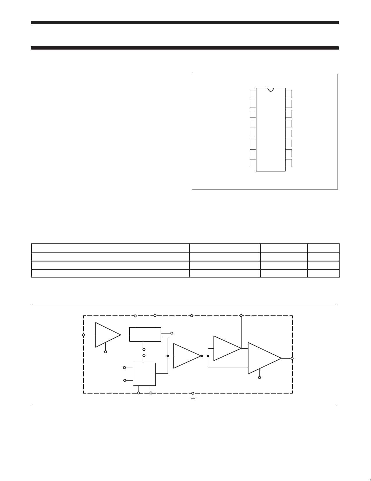
BLOCK DIAGRAM
45
LIMITER
6
PHASE
COMPARATOR
3
7
11
9
VCO
10
12 13
V+
1 14
2
AMPLIFIER
DC
RETRIEVER
SCHMITT
TRIGGER
POST DETECTION
PROCESSOR
8
15
Figure 2. Block Diagram
16
SR01026
1994 Aug 31
1 853-0908 13720
1 page 
Philips Semiconductors
Phase-locked loop
Product specification
NE/SE564
FUNCTIONAL DESCRIPTION
(Figure 6)
The NE564 is a monolithic phase-locked loop with a post detection
processor. The use of Schottky clamped transistors and optimized
device geometries extends the frequency of operation to greater
than 50MHz.
In addition to the classical PLL applications, the NE564 can be used
as a modulator with a controllable frequency deviation.
The output of the PLL can be written as shown in the following
equation:
VO =
(fIN - fO)
KVCO
(1)
KVCO = conversion gain of the VCO
fIN = frequency of the input signal
fO = free-running frequency of the VCO
The process of recovering FSK signals involves the conversion of
the PLL output into logic compatible signals. For high data rates, a
considerable amount of carrier will be present at the output of the
PLL due to the wideband nature of the loop filter. To avoid the use
of complicated filters, a comparator with hysteresis or Schmitt trigger
is required. With the conversion gain of the VCO fixed, the output
voltage as given by Equation 1 varies according to the frequency
deviation of fIN from fO. Since this differs from system to system, it
is necessary that the hysteresis of the Schmitt trigger be capable of
being changed, so that it can be optimized for a particular system.
This is accomplished in the 564 by varying the voltage at Pin 15
which results in a change of the hysteresis of the Schmitt trigger.
For FSK signals, an important factor to be considered is the drift in
the free-running frequency of the VCO itself. If this changes due to
temperature, according to Equation 1 it will lead to a change in the
DC levels of the PLL output, and consequently to errors in the digital
output signal. This is especially true for narrowband signals where
the deviation in fIN itself may be less than the change in fO due to
temperature. This effect can be eliminated if the DC or average
value of the signal is retrieved and used as the reference to the
comparator. In this manner, variations in the DC levels of the PLL
output do not affect the FSK output.
VCO Section
Due to its inherent high-frequency performance, an emitter-coupled
oscillator is used in the VCO. In the circuit, shown in the equivalent
schematic, transistors Q21 and Q23 with current sources Q25 - Q26
form the basic oscillator. The approximate free-running frequency of
the oscillator is shown in the following equation:
1
fO ≅ 22 RC (C1 + CS)
(2)
RC = R19 = R20 = 100Ω (INTERNAL)
C1 = external frequency setting capacitor
CS = stray capacitance
Variation of VD (phase detector output voltage) changes the
frequency of the oscillator. As indicated by Equation 2, the
frequency of the oscillator has a negative temperature coefficient
due to the monolithic resistor. To compensate for this, a current IR
with negative temperature coefficient is introduced to achieve a low
frequency drift with temperature.
Phase Comparator Section
The phase detection processor consists of a doubled-balanced
modulator with a limiter amplifier to improve AM rejection.
Schottky-clamped vertical PNPs are used to obtain TTL level inputs.
The loop gain can be varied by changing the current in Q4 and Q15
which effectively changes the gain of the differential amplifiers. This
can be accomplished by introducing a current at Pin 2.
Post Detection Processor Section
The post detection processor consists of a unity gain
transconductance amplifier and comparator. The amplifier can be
used as a DC retriever for demodulation of FSK signals, and as a
post detection filter for linear FM demodulation. The comparator has
adjustable hysteresis so that phase jitter in the output signal can be
eliminated.
As shown in the equivalent schematic, the DC retriever is formed by
the transconductance amplifier Q42 - Q43 together with an external
capacitor which is connected at the amplifier output (Pin 14). This
forms an integrator whose output voltage is shown in the following
equation:
VO =
gM
C2
VINdt
(3)
gM = transconductance of the amplifier
C2 = capacitor at the output (Pin 14)
VIN = signal voltage at amplifier input
With proper selection of C2, the integrator time constant can be
varied so that the output voltage is the DC or average value of the
input signal for use in FSK, or as a post detection filter in linear
demodulation.
The comparator with hysteresis is made up of Q49 - Q50 with
positive feedback being provided by Q47 - Q48. The hysteresis is
varied by changing the current in Q52 with a resulting variation in the
loop gain of the comparator. This method of hysteresis control,
which is a DC control, provides symmetric variation around the
nominal value.
Design Formula
The free-running frequency of the VCO is shown by the following
equation:
fO ≅
1
22 RC (C1 + CS)
(4)
RC = 100Ω
C1 = external cap in farads
CS = stray capacitance
The loop filter diagram shown is explained by the following equation:
1
fS = 1 + sRC3 (First Order)
(5)
R = R12 = R13 = 1.3kΩ (Internal)*
By adding capacitors to Pins 4 and 5, a pole is added to the loop
transfer at
1
ω = RC3
NOTE:
*Refer to Figure 6.
1994 Aug 31
5
5 Page | ||
| Páginas | Total 9 Páginas | |
| PDF Descargar | [ Datasheet SE564.PDF ] | |
Hoja de datos destacado
| Número de pieza | Descripción | Fabricantes |
| SE564 | Phase-locked loop | Philips |
| SE565 | Phase-Lock Loop | ETC |
| SE566 | Function generator | Philips |
| SE567 | Tone decoder/phase-locked loop | Philips |
| Número de pieza | Descripción | Fabricantes |
| SLA6805M | High Voltage 3 phase Motor Driver IC. |
Sanken |
| SDC1742 | 12- and 14-Bit Hybrid Synchro / Resolver-to-Digital Converters. |
Analog Devices |
|
DataSheet.es es una pagina web que funciona como un repositorio de manuales o hoja de datos de muchos de los productos más populares, |
| DataSheet.es | 2020 | Privacy Policy | Contacto | Buscar |