|
|
PDF OPA699 Data sheet ( Hoja de datos )
| Número de pieza | OPA699 | |
| Descripción | Wideband / High Gain VOLTAGE LIMITING AMPLIFIER | |
| Fabricantes | Burr-Brown | |
| Logotipo |  |
|
Hay una vista previa y un enlace de descarga de OPA699 (archivo pdf) en la parte inferior de esta página. Total 25 Páginas | ||
|
No Preview Available !
OPA699
OPA699
SBOS261B – NOVEMBER 2002 – REVISED OCTOBER 2003
Wideband, High Gain
VOLTAGE LIMITING AMPLIFIER
FEATURES
q HIGH LINEARITY NEAR LIMITING
q FAST RECOVERY FROM OVERDRIVE: 1ns
q LIMITING VOLTAGE ACCURACY: ±10mV
q –3dB BANDWIDTH (G = +6): 260MHz
q GAIN BANDWIDTH PRODUCT: 1000MHz
q STABLE FOR G ≥ +4V/V
q SLEW RATE: 1400V/µs
q ±5V AND +5V SUPPLY OPERATION
q LOW GAIN VERSION: OPA698
APPLICATIONS
q TRANSIMPEDANCE WITH FAST
OVERDRIVE RECOVERY
q FAST LIMITING ADC INPUT DRIVER
q LOW PROP DELAY COMPARATOR
q NONLINEAR ANALOG SIGNAL
PROCESSING
q DIFFERENCE AMPLIFIER
q IF LIMITING AMPLIFIER
q OPA689 UPGRADE
DESCRIPTION
The OPA699 is a wideband, voltage-feedback op amp that
offers bipolar output voltage limiting, and is stable for gains
≥ +4. Two buffered limiting voltages take control of the output
when it attempts to drive beyond these limits. This new
output limiting architecture holds the limiter offset error to
±10mV. The op amp operates linearly to within 20mV of the
limits.
The combination of narrow nonlinear range and low limiting
offset allows the limiting voltages to be set within 100mV of
the desired linear output range. A fast 1ns recovery from
limiting ensures that overdrive signals will be transparent to
the signal channel. Implementing the limiting function at the
output, as opposed to the input, gives the specified limiting
accuracy for any gain, and allows the OPA699 to be used in
all standard op amp applications.
Nonlinear analog signal processing circuits will benefit from
the OPA699 sharp transition from linear operation to output
limiting. The quick recovery time supports high-speed applica-
tions.
The OPA699 is available in an industry-standard pinout in an
SO-8 package. For lower gain applications requiring output
limiting with fast recovery, consider the OPA698.
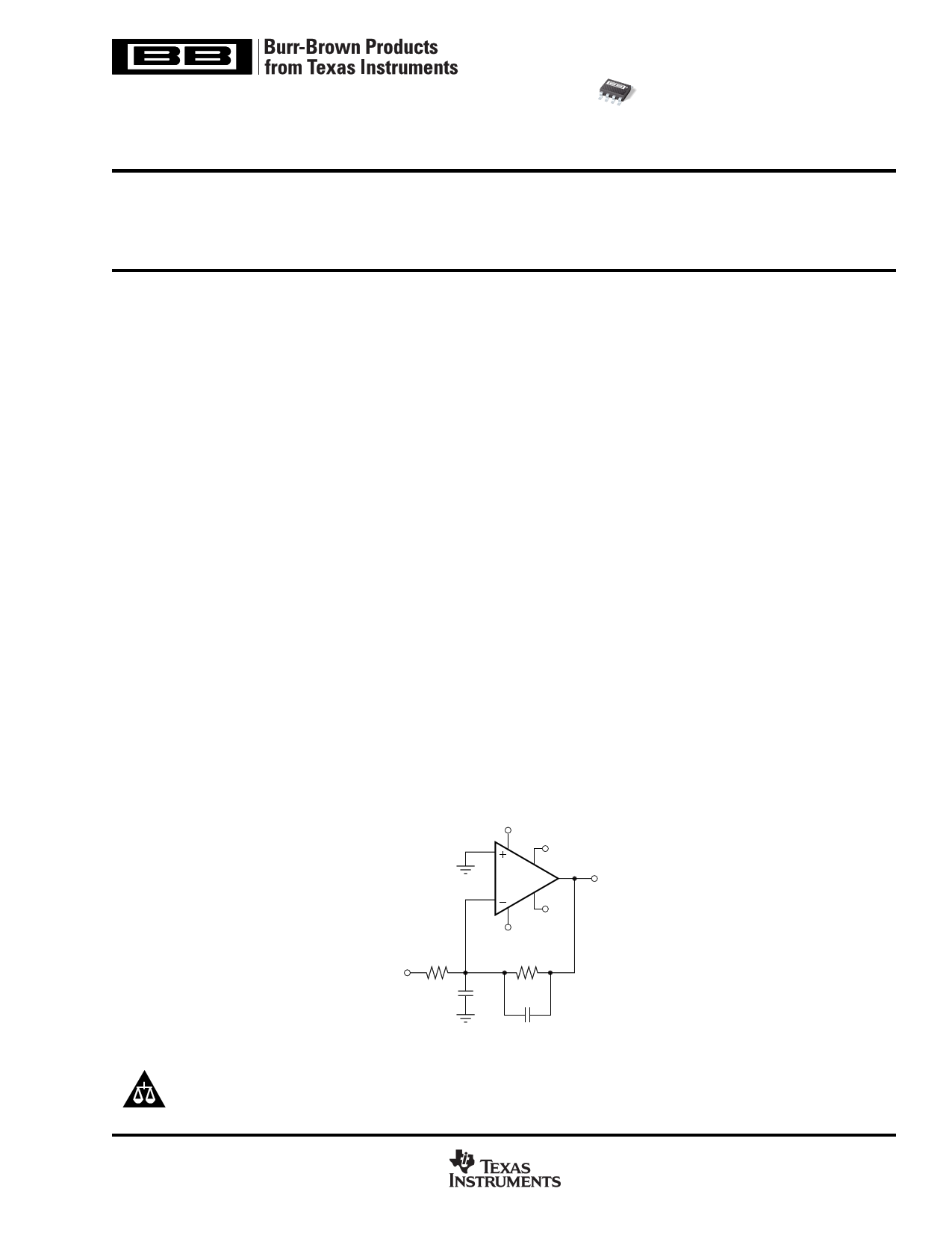
RG
374Ω
VIN
+5V
VH
OPA699
VL
–5V
RF
750Ω
VOUT
VOUT = –2VIN
CS
18pF
CF
4pF
Low Gain, Improved SFDR Amplifier with Output Limiting
Please be aware that an important notice concerning availability, standard warranty, and use in critical applications of
Texas Instruments semiconductor products and disclaimers thereto appears at the end of this data sheet.
All trademarks are the property of their respective owners.
PRODUCTION DATA information is current as of publication date.
Products conform to specifications per the terms of Texas Instruments
standard warranty. Production processing does not necessarily include
testing of all parameters.
www.ti.com
Copyright © 2002-2003, Texas Instruments Incorporated
1 page 
ELECTRICAL CHARACTERISTICS: VS = +5V
Boldface limits are tested at +25°C.
G = +6, RF = 750Ω, RL = 500Ω tied to VCM = +2.5V, VL = VCM –1.2V, and VH = VCM +1.2V, (see Figure 2 for AC performance only), unless otherwise noted.
TYP
OPA699ID
MIN/MAX OVER TEMPERATURE
PARAMETER
CONDITIONS
+25°C
+25°C(1)
0°C to
70°C(2)
–40°C to
+85°C(2)
MIN/ TEST
UNITS MAX LEVEL(3)
AC PERFORMANCE (see Figure 2)
Small Signal Bandwidth (VO < 0.5VPP)
Gain Bandwidth Product (G ≥ +20)
Gain Peaking
0.1dB Gain Flatness Bandwidth
Large-Signal Bandwidth
Step Response
Slew Rate
Rise-and-Fall Time
Settling Time: 0.05%
Spurious-Free Dynamic Range, Even
Odd
Input Noise
Voltage Noise Density
Current Noise Density
DC PERFORMANCE
Open-Loop Voltage Gain (AOL)
Input Offset Voltage
Average Drift
Input Bias Current(4)
Average Drift
Input Offset Current
Average Drift
INPUT
Common-Mode Rejection Ratio
Common-Mode Input Range(5)
Input Impedance
Differential-Mode
Common-Mode
OUTPUT
Output Voltage Range
Current Output, Sourcing
Sinking
Closed-Loop Output Impedance
POWER SUPPLY
Operating Voltage, Specified
Maximum
Quiescent Current, Maximum
Minimum
Power-Supply Rejection Ratio
+PSRR (Input Referred)
G = +6
G = +12
G = –6
VO < 0.5VPP
VO < 0.5VPP, G = +4
VO < 0.5VPP, G = +6
VO = 2VPP
2V Step
0.5V Step
2V Step
f = 5MHz, VO = 2VPP
f = 5MHz, VO = 2VPP
f ≥ 1MHz
f ≥ 1MHz
VO = VCM ± 0.5V
Input Referred, VCM ±0.5V
VH = VCM + 1.8V, VL = VCM – 1.8V
RL ≥ 500Ω
G = +4, f < 100kHz
VS = +5V
VS = +5V
VS = 4.5V to 5.5V
234 200 190 180 MHz min B
83
MHz
typ C
242
MHz
typ C
880 700 650 600 MHz min B
8 dB typ C
30
MHz
typ C
250 200 190 180 MHz min B
1050
850
800
700 V/µs min B
1.75
1.8
1.9
2.1
ns max B
8 ns typ C
64 61 60 58 dB min B
70 69 67 65 dB min B
4.2 4.6 5.2 5.6 nV/√Hz max B
2.1 2.6 2.8 3.0 pA/√Hz max B
66 56 54 53 dB min A
±2 ±6 ±7 ±8 mV max A
— ±14 ±14 µV/°C max B
+3 ±10 ±11 ±12 µA max A
— ±25 ±25 nA/°C max B
±0.4 ±2 ±2.5 ±3
µA max A
— ±15 ±15 nA/°C max B
58
VCM ±0.8
0.32 || 1
3.5 || 1
54
VCM ±0.7
53
VCM ±0.7
52
VCM ±0.6
dB
V
MΩ || pF
MΩ || pF
min
min
typ
typ
A
A
C
C
VCM ±1.6
+70
–70
0.2
VCM ±1.4
+60
–60
VCM ±1.4
+55
–55
VCM ±1.3
+50
–50
V
mA
mA
Ω
min A
min A
min A
typ C
5
— +12 +12 +12
14.3 14.9 15.1 15.3
14.3 13.6 13.4 13.2
70
V typ C
V max A
mA max A
mA min A
dB typ C
NOTES: (1) Junction temperature = ambient temperature for low temperature limit and +25°C Test Level A specifications. Junction temperature = ambient
temperature +23°C at high temperature limit Test Level A specifications.
(2) Junction temperature = ambient at low temperature limit; junction temperature = ambient +1°C at high temperature limit for over-temperature
tested specifications.
(3) Test Levels: (A) 100% tested at +25°C. Over temperature limits by characterization and simulation. (B) Limits set by characterization and
simulation. (C) Typical value for information only.
(4) Current is considered positive out of node.
(5) CMIR tested as < 3dB degradation from minimum CMRR at specified limits.
(6) IVH (VH bias current) is negative, and IVL (VL bias current) is positive, under these conditions. See Note 3 and Figures 2 and 12.
(7) Limiter feedthrough is the ratio of the output magnitude to the sinewave added to VH (or VL) when VIN = 0.
(8) VH slew rate conditions are: VIN = VCM +0.4V, G = +6, VL = VCM –1.2V, VH = step between VCM +1.2V and VCM. VL slew rate conditions are similar.
(9) Linearity Guardband is defined for an output sinusoid (f = 5MHz, VO = VCM ±1VPP) centered between the limiter levels (VH and VL). It is the
difference between the limiter level and the peak output voltage where SFDR decreases by 3dB (see Figure 8).
OPA699
SBOS261B
www.ti.com
5
5 Page 
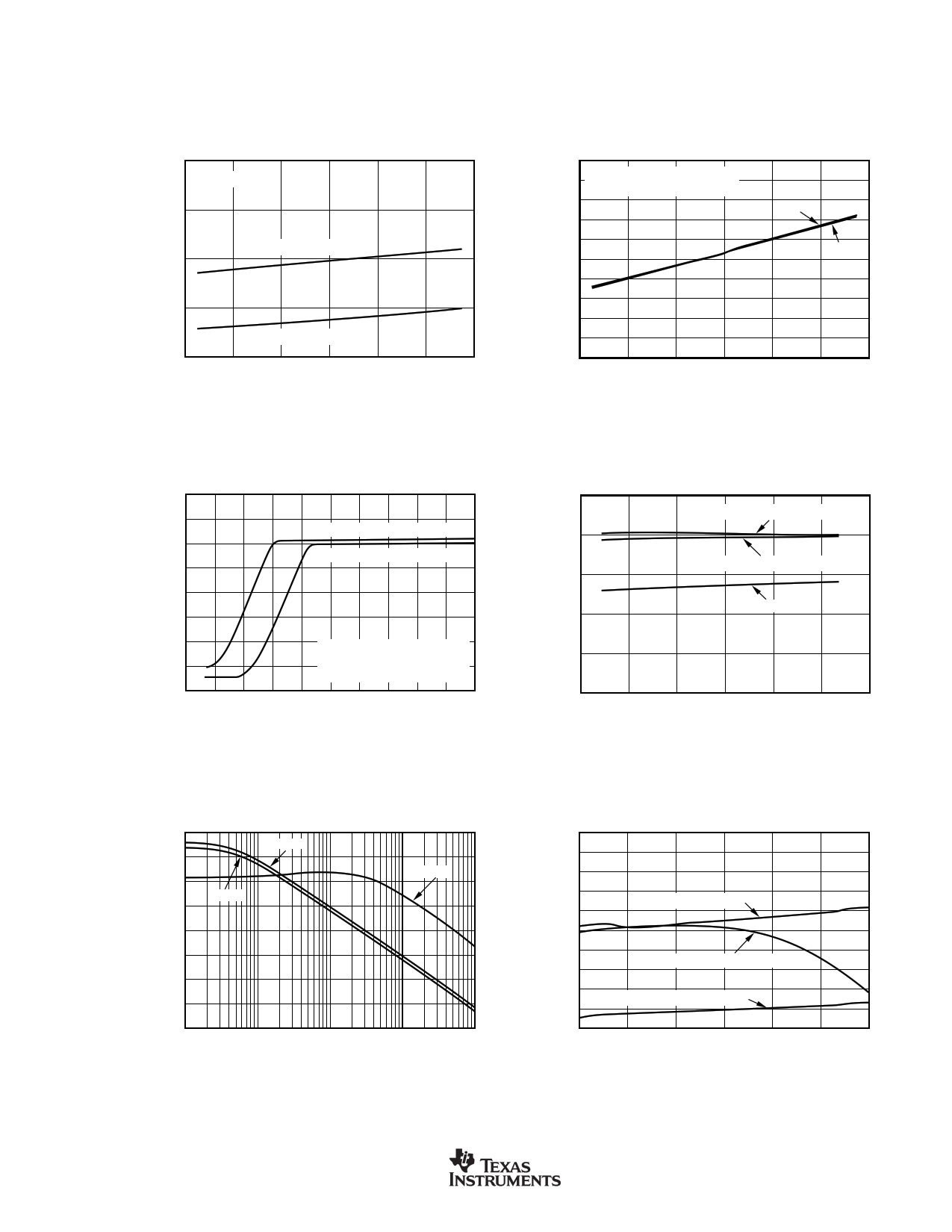
TYPICAL CHARACTERISTICS: VS = ±5V (Cont.)
TA = +25°C, G = +6, RF = 750Ω, and RL = 500Ω, VH = –VL = 2V, unless otherwise noted.
VOLTAGE RANGES vs TEMPERATURE
5.0
VH = –VL = 4.3V
4.5
Output Voltage Range
4.0
3.5
3.0
−50
Common-Mode Input Range
−25 0
25 50
Ambient Temperature (°C)
75
100
LIMITED VOLTAGE RANGE vs TEMPERATURE
4.0
3.9 VH and VL left open
Internal Default Limited Voltage
3.8
3.7
VH
3.6
3.5 VL
3.4
3.3
3.2
3.1
3.0
−50
−25 0
25 50 75
Ambient Temperature (°C)
100
LIMITER INPUT BIAS CURRENT vs BIAS VOLTAGE
100
75
Maximum Over Temperature
50
Minimum Over Temperature
25
0
–25
–50
–75
–100
0
Limiter Headroom = +VS – VH
= VL – (–VS)
Current = IVH or –IVL
0.5 1.0 1.5 2.0 2.5 3.0 3.5 4.0 4.5 5.0
Limiter Headroom (V)
SUPPLY AND OUTPUT CURRENTS
vs TEMPERATURE
20 100
Output Current, Sinking
18 98
Output Current, Sourcing
16 96
Supply Current
14 94
12 92
10
–50
–25 0
25 50
Ambient Temperature (°C)
75
90
100
COMMON-MODE REJECTION RATIO AND
POWER-SUPPLY REJECTION vs FREQUENCY
80
–PSRR
70
CMRR
60
+PSRR
50
40
30
20
10
0
10k
100k
1M
Frequency (Hz)
10M
100M
4.5
4.0
3.5
3.0
2.5
2.0
1.5
1.0
0.5
0
–0.5
−50
TYPICAL DRIFT OVER TEMPERATURE
Input Bias Current (IB)
Input Offset Voltage (VOS)
Input Offset Current (IOS)
−25 0 25 50 75
Ambient Temperature (°C)
1
0.9
0.8
0.7
0.6
0.5
0.4
0.3
0.2
0.1
0
100
OPA699
SBOS261B
www.ti.com
11
11 Page | ||
| Páginas | Total 25 Páginas | |
| PDF Descargar | [ Datasheet OPA699.PDF ] | |
Hoja de datos destacado
| Número de pieza | Descripción | Fabricantes |
| OPA690 | Wideband Voltage-Feedback Operational Amplifier with Disable (Rev. F) | Texas Instruments |
| OPA690 | Low-Power / Single-Supply / Wideband Operational Amplifier | Burr-Brown |
| OPA691 | Wideband Current Feedback Operational Amplifier With Disable (Rev. D) | Texas Instruments |
| OPA691 | Quad / Low-Power / Current-Feedback OPERATIONAL AMPLIFIER | Burr-Brown |
| Número de pieza | Descripción | Fabricantes |
| SLA6805M | High Voltage 3 phase Motor Driver IC. |
Sanken |
| SDC1742 | 12- and 14-Bit Hybrid Synchro / Resolver-to-Digital Converters. |
Analog Devices |
|
DataSheet.es es una pagina web que funciona como un repositorio de manuales o hoja de datos de muchos de los productos más populares, |
| DataSheet.es | 2020 | Privacy Policy | Contacto | Buscar |
