|
|
|
PDF OPA658 Data sheet ( Hoja de datos )
| Número de pieza | OPA658 | |
| Descripción | Wideband / Low Power Current Feedback OPERATIONAL AMPLIFIER | |
| Fabricantes | Burr-Brown | |
| Logotipo | ||
Hay una vista previa y un enlace de descarga de OPA658 (archivo pdf) en la parte inferior de esta página. Total 13 Páginas | ||
|
No Preview Available !
® OPA658
OPA658
OPA658
Wideband, Low Power Current Feedback
OPERATIONAL AMPLIFIER
FEATURES
q UNITY GAIN STABLE BANDWIDTH:
900MHz
q LOW POWER: 50mW
q LOW DIFFERENTIAL GAIN/PHASE ERRORS:
0.025%/0.02°
q HIGH SLEW RATE: 1700V/µs
q GAIN FLATNESS: 0.1dB to 135MHz
q HIGH OUTPUT CURRENT (80mA)
APPLICATIONS
q MEDICAL IMAGING
q HIGH-RESOLUTION VIDEO
q HIGH-SPEED SIGNAL PROCESSING
q COMMUNICATIONS
q PULSE AMPLIFIERS
q ADC/DAC GAIN AMPLIFIER
q MONITOR PREAMPLIFIER
q CCD IMAGING AMPLIFIER
DESCRIPTION
The OPA658 is an ultra-wideband, low power current
feedback video operational amplifier featuring high
slew rate and low differential gain/phase error. The
current feedback design allows for superior large sig-
nal bandwidth, even at high gains. The low differential
gain/phase errors, wide bandwidth and low quiescent
current make the OPA658 a perfect choice for numer-
ous video, imaging and communications applications.
The OPA658 is optimized for low gain operation and
is also available in dual (OPA2658) and quad
(OPA4658) configurations.
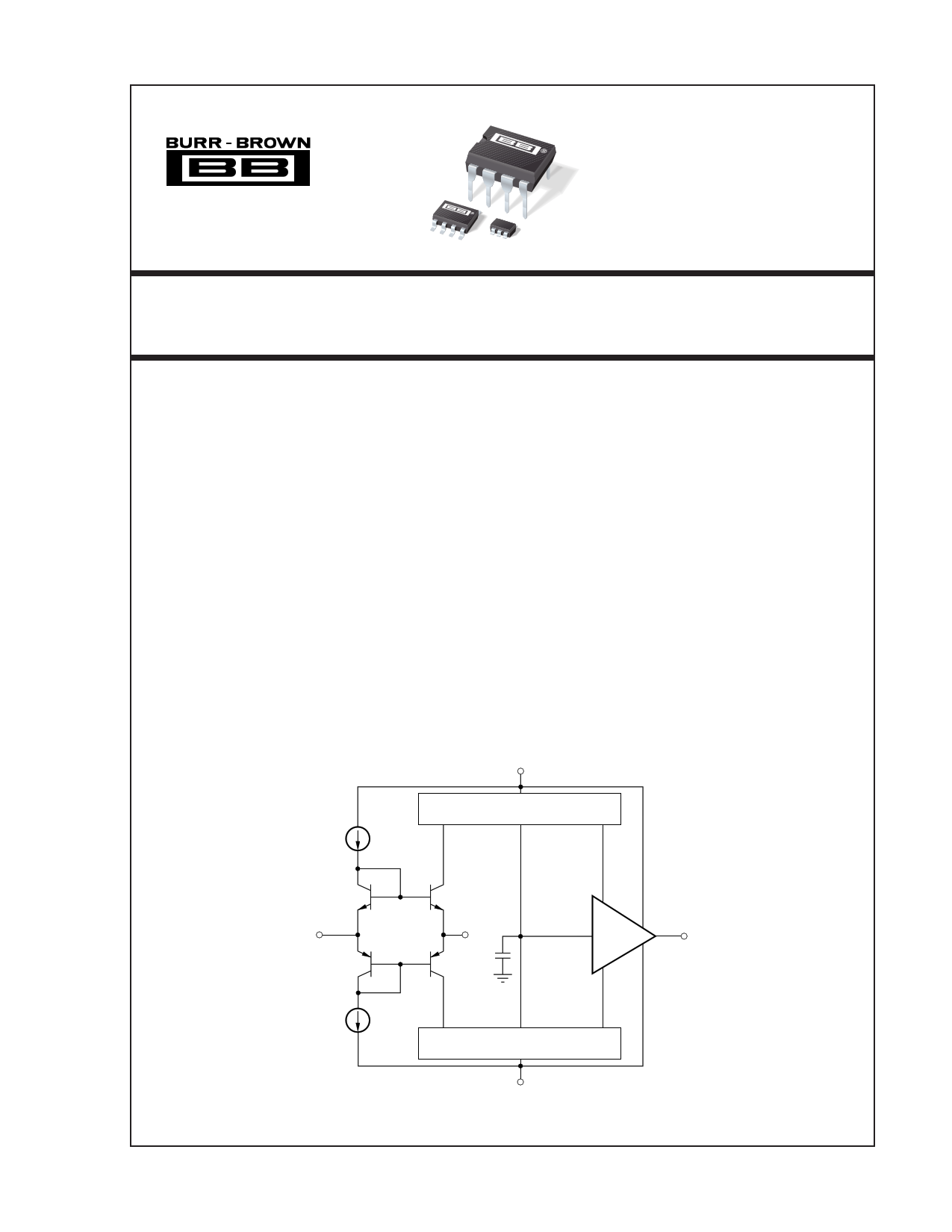
+VS
IBIAS
Current Mirror
In+
In–
Buffer
VOUT
CCOMP
IBIAS
Current Mirror
–VS
International Airport Industrial Park • Mailing Address: PO Box 11400, Tucson, AZ 85734 • Street Address: 6730 S. Tucson Blvd., Tucson, AZ 85706 • Tel: (520) 746-1111 • Twx: 910-952-1111
Internet: http://www.burr-brown.com/ • FAXLine: (800) 548-6133 (US/Canada Only) • Cable: BBRCORP • Telex: 066-6491 • FAX: (520) 889-1510 • Immediate Product Info: (800) 548-6132
© 1994 Burr-Brown Corporation
PDS-11268F
OPA658Printed in U.S.A. March, 1998
®
1 page 
TYPICAL PERFORMANCE CURVES (CONT)
At TA = +25°C, VS = ±5V, RL = 100Ω, and RFB = 402Ω, unless otherwise noted.
INVERTING INPUT BIAS CURRENT
vs TEMPERATURE
2.0
1.8
1.6
1.4
1.2
1.0
0.8
0.6
0.4
–75 –50 –25
0
25 50 75 100 125
Temperature (°C)
106
105
104
103
102
101
1
1k
OPEN-LOOP TRANSIMPEDANCE AND PHASE
vs FREQUENCY
Transimpedance
0
Phase
–45
–90
–135
–180
–225
10k 100k 1M
10M 100M 1G
Frequency (Hz)
OPEN-LOOP GAIN AND PHASE vs FREQUENCY
60
40
Gain
0
Phase
20 –45
0 –90
–20 –135
–40 –180
–60
1k
–225
10k 100k 1M 10M 100M 1G
Frequency (Hz)
CLOSED-LOOP BANDWIDTH
6
SO-8 Bandwidth = 881MHz, RFB = 402Ω
3
G = +1
0
–3
DIP Bandwidth = 949MHz, RFB = 560Ω
–6
–9
1M
10M 100M
Frequency (Hz)
1G
9
6
3
0
–3
–6
1M
CLOSED-LOOP BANDWIDTH
G = +2
DIP Bandwidth = 682MHz
SO-8 Bandwidth = 680MHz
10M 100M
Frequency (Hz)
1G
20
17
14
11
8
5
2
1M
CLOSED-LOOP BANDWIDTH
G = +5
SO-8/DIP Bandwidth= 372MHz
10M 100M
Frequency (Hz)
1G
®
5 OPA658
5 Page 
402Ω
402Ω
OPA658
10Ω to 35Ω
RISO
50Ω
RL CL
FIGURE 5. Driving Capacitive Loads.
COMPENSATION
The OPA658 is internally compensated and is stable in unity
gain with a phase margin of approximately 62°, and approxi-
mately 64° in a gain of +2V/V when used with the recom-
mended feedback resistor value. Frequency response for
other gains are shown in the Typical Performance Curves.
The high-frequency response of the OPA658 in a good
layout is very flat with frequency.
DISTORTION
The OPA658’s Harmonic Distortion characteristics into a
100Ω load are shown versus frequency and power output in
the Typical Performance Curves. Distortion can be further
improved by increasing the load resistance as illustrated in
Figure 6. Remember to include the contribution of the
feedback resistance when calculating the effective load re-
sistance seen by the amplifier.
5MHz HARMONIC DISTORTION vs
LOAD RESISTANCE (G = +2)
–55
–60
G = +2, VO = 2Vp-p, fO = 5MHz
–65
3fO
–70
–75
–80 2fO
–85
10
100
Load Resistance (Ω)
1k
FIGURE 6. 5MHz Harmonic Distortion vs Load Resistance.
Narrowband communication channel requirements will ben-
efit from the OPA658’s wide bandwidth and low
intermodulation distortion on low quiescent power. If output
signal power at two closely spaced frequencies is required,
third-order nonlinearities in any amplifier will cause spuri-
ous power at frequencies very near the two funda-
mental frequencies. If the two test frequencies, f1 and f2,
are specified in terms of average and delta frequency,
fO = (f1 + f2)/2 and ∆f = f2 – f1, the two, third-order,
close-in spurious tones will appear at fO ±3 • ∆f. The two
tone, third-order spurious plot shown in Figure 7 indicates
how far below these two equal power, closely spaced, tones
the intermodulation spurious will be. The single tone power
is at a matched 50Ω load. The unique design of the OPA658
provides much greater spurious free range than what a two-
tone third-order intermodulation intercept specification would
predict. This can be seen in Figure 7 as the spurious free
range actually increases at the higher output power levels.
TWO TONE, THIRD-ORDER SPURIOUS LEVELS
–65
20MHz
–70
–75 10MHz
–80 5MHz
–85
–90
–18 –16 –14 –12 –10 –8 –6 –4 –2 0 2 4
Single Tone Power (dBm)
FIGURE 7. Third-Order Spurious Level vs Frequency.
DIFFERENTIAL GAIN AND PHASE
Differential Gain (dG) and Differential Phase (dP) are among
the more important specifications for video applications. dG
is defined as the percent change in closed-loop gain over a
specified change in output voltage level. dP is defined as the
change in degrees of the closed-loop phase over the same
output voltage change. Both dG and dP are specified at the
NTSC sub-carrier frequency of 3.58MHz and the PAL sub-
carrier of 4.43MHz. All NTSC measurements were per-
formed using a Tektronix model VM700A Video Measure-
ment Set.
dG/dP of the OPA658 were measured with the amplifier in a
gain of +2V/V with 75Ω input impedance and the output
back-terminated in 75Ω. The input signal selected from the
generator was a 0V to 1.4V modulated ramp with sync pulse.
With these conditions the test circuit shown in Figure 8
delivered a 100IRE modulated ramp to the 75Ω input of the
videoanalyzer. The signal averaging feature of the analyzer
75Ω
OPA658
75Ω 402Ω
TEK TSG 130A
402Ω
75Ω
75Ω
TEK VM700A
FIGURE 8. Configuration for Testing Differential Gain/Phase.
®
11 OPA658
11 Page | ||
| Páginas | Total 13 Páginas | |
| PDF Descargar | [ Datasheet OPA658.PDF ] | |
Hoja de datos destacado
| Número de pieza | Descripción | Fabricantes |
| OPA650 | Wideband Low Power Voltage Feedback Operational Amplifier | Texas Instruments |
| OPA650 | Wideband / Low Power Voltage Feedback OPERATIONAL AMPLIFIER | Burr-Brown |
| OPA651 | Wideband / Low Power Voltage Feedback OPERATIONAL AMPLIFIER | Burr-Brown |
| OPA653 | Wideband Fixed Gain JFET-Input Amplifier (Rev. A) | Texas Instruments |
| Número de pieza | Descripción | Fabricantes |
| SLA6805M | High Voltage 3 phase Motor Driver IC. |
Sanken |
| SDC1742 | 12- and 14-Bit Hybrid Synchro / Resolver-to-Digital Converters. |
Analog Devices |
|
DataSheet.es es una pagina web que funciona como un repositorio de manuales o hoja de datos de muchos de los productos más populares, |
| DataSheet.es | 2020 | Privacy Policy | Contacto | Buscar |