|
|
PDF OPA657 Data sheet ( Hoja de datos )
| Número de pieza | OPA657 | |
| Descripción | 1.6GHz / Low-Noise / FET-Input OPERATIONAL AMPLIFIER | |
| Fabricantes | Brilliance Semiconductor | |
| Logotipo | ||
Hay una vista previa y un enlace de descarga de OPA657 (archivo pdf) en la parte inferior de esta página. Total 20 Páginas | ||
|
No Preview Available !
OPA657
OPA657
SBOS197B – DECEMBER 2001 – REVISED MAY 2004
1.6GHz, Low-Noise, FET-Input
OPERATIONAL AMPLIFIER
FEATURES
q HIGH GAIN BANDWIDTH PRODUCT: 1.6GHz
q HIGH BANDWIDTH 275MHz (G = +10)
q LOW INPUT OFFSET VOLTAGE: ±0.25mV
q LOW INPUT BIAS CURRENT: 2pA
q LOW INPUT VOLTAGE NOISE: 4.8nV/ Hz
q HIGH OUTPUT CURRENT: 70mA
q FAST OVERDRIVE RECOVERY
APPLICATIONS
q WIDEBAND PHOTODIODE AMPLIFIER
q WAFER SCANNING EQUIPMENT
q ADC INPUT AMPLIFIER
q TEST AND MEASUREMENT FRONT END
q HIGH GAIN PRECISION AMPLIFIER
DESCRIPTION
The OPA657 combines a high gain bandwidth, low distor-tion,
voltage-feedback op amp with a low voltage noise JFET-input
stage to offer a very high dynamic range amplifier for high
precision ADC (Analog-to-Digital Converter) driving or wideband
transimpedance applications. Photodiode applications will see
improved noise and bandwidth using this decompensated,
high gain bandwidth amplifier.
Very low level signals can be significantly amplified in a single
OPA657 gain stage with exceptional bandwidth and accuracy.
Having a high 1.6GHz gain bandwidth product will give >
10MHz signal bandwidths up to gains of 160V/V (44dB). The
very low input bias current and capacitance will support this
performance even for relatively high source impedances.
Broadband photodetector applications will benefit from the low
voltage noise JFET inputs for the OPA657. The JFET input
contributes virtually no current noise while for broadband
applications, a low voltage noise is also required. The low
4.8nV/ Hz input voltage noise will provide exceptional input
sensitivity for higher bandwidth applications. The example
shown below will give a total equivalent input noise current of
1.8pA/ Hz over a 10MHz bandwidth.
200kΩ TRANSIMPEDANCE BANDWIDTH
116
10MHz Bandwidth
106
96
86
RELATED OPERATIONAL AMPLIFIER PRODUCTS
SLEW VOLTAGE
VS BW RATE NOISE
DEVICE (V) (MHz) (V/µS) (nV/√HZ) AMPLIFIER DESCRIPTION
OPA355 +5
OPA655 ±5
OPA656 ±5
OPA627 ±15
THS4601 ±15
200
400
500
16
180
300
290
170
55
100
5.80
6
7
4.5
5.4
Unity-Gain Stable CMOS
Unity-Gain Stable FET-Input
Unity-Gain Stable FET-Input
Unity-Gain Stable FET-Input
Unity-Gain Stable FET-Input
76 0.1pF
66
100kHz
1MHz
Frequency
10MHz
50MHz
200kΩ
λ
OPA657
VO
(12pF)
–Vb
Wideband Photodiode Transimpedance Amplifier
Please be aware that an important notice concerning availability, standard warranty, and use in critical applications of
Texas Instruments semiconductor products and disclaimers thereto appears at the end of this data sheet.
All trademarks are the property of their respective owners.
PRODUCTION DATA information is current as of publication date.
Products conform to specifications per the terms of Texas Instruments
standard warranty. Production processing does not necessarily include
testing of all parameters.
www.ti.com
Copyright © 2001-2004, Texas Instruments Incorporated
1 page 
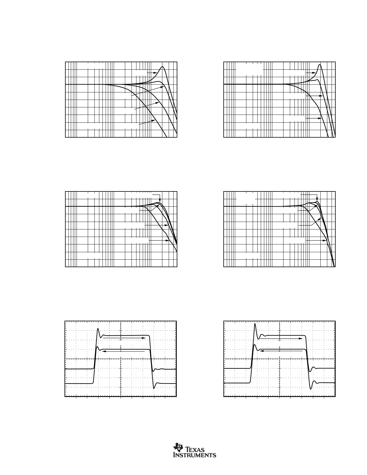
TYPICAL CHARACTERISTICS: VS = ±5V
TA = +25°C, G = +10, RF = 453Ω, RL = 100Ω, unless otherwise noted.
9
6
3
0
–3
–6
–9
–12
–15
–18
–21
0.5
NONINVERTING SMALL-SIGNAL
FREQUENCY RESPONSE
VO = 0.2Vp-p
G = +7
See Figure 1
G = +10
G = +20
G = +50
1 10 100
Frequency (MHz)
500
9
6
3
0
–3
–6
–9
–12
–15
–18
–21
0.5
INVERTING SMALL-SIGNAL
FREQUENCY RESPONSE
VO = 0.2Vp-p
RG = 50Ω
G = –12
G = –20
See Figure 2
G = –50
1 10 100
Frequency (MHz)
500
26
23
20
17
14
11
8
5
2
–1
–4
0.5
NONINVERTING LARGE-SIGNAL
FREQUENCY RESPONSE
G = +10
VO = 0.2Vp-p
VO = 1Vp-p
VO = 2Vp-p
VO = 5Vp-p
See Figure 1
1 10 100
Frequency (MHz)
500
32
29
26
23
20
17
14
11
8
5
2
0.5
INVERTING LARGE-SIGNAL
FREQUENCY RESPONSE
G = –20
RF = 1kΩ
VO = 0.2Vp-p
VO = 1Vp-p
VO = 1Vp-p
VO = 5Vp-p
See Figure 2
1 10 100
Frequency (MHz)
500
0.8
0.6
0.4
0.2
0
–0.2
–0.4
–0.6
–0.8
NONINVERTING PULSE RESPONSE
G = +10
Large-Signal Right Scale
Small-Signal Left Scale
See Figure 1
Time (10ns/div)
1.6
1.2
0.8
0.4
0
–0.4
–0.8
–1.2
–1.6
INVERTING PULSE RESPONSE
0.8
G = –20
0.6
0.4
Large-Signal Right Scale
0.2
Small-Signal Left Scale
0
–0.2
–0.4
–0.6
See Figure 2
–0.8
Time (10ns/div)
1.6
1.2
0.8
0.4
0
–0.4
–0.8
–1.2
–1.6
OPA657
SBOS197B
www.ti.com
5
5 Page 
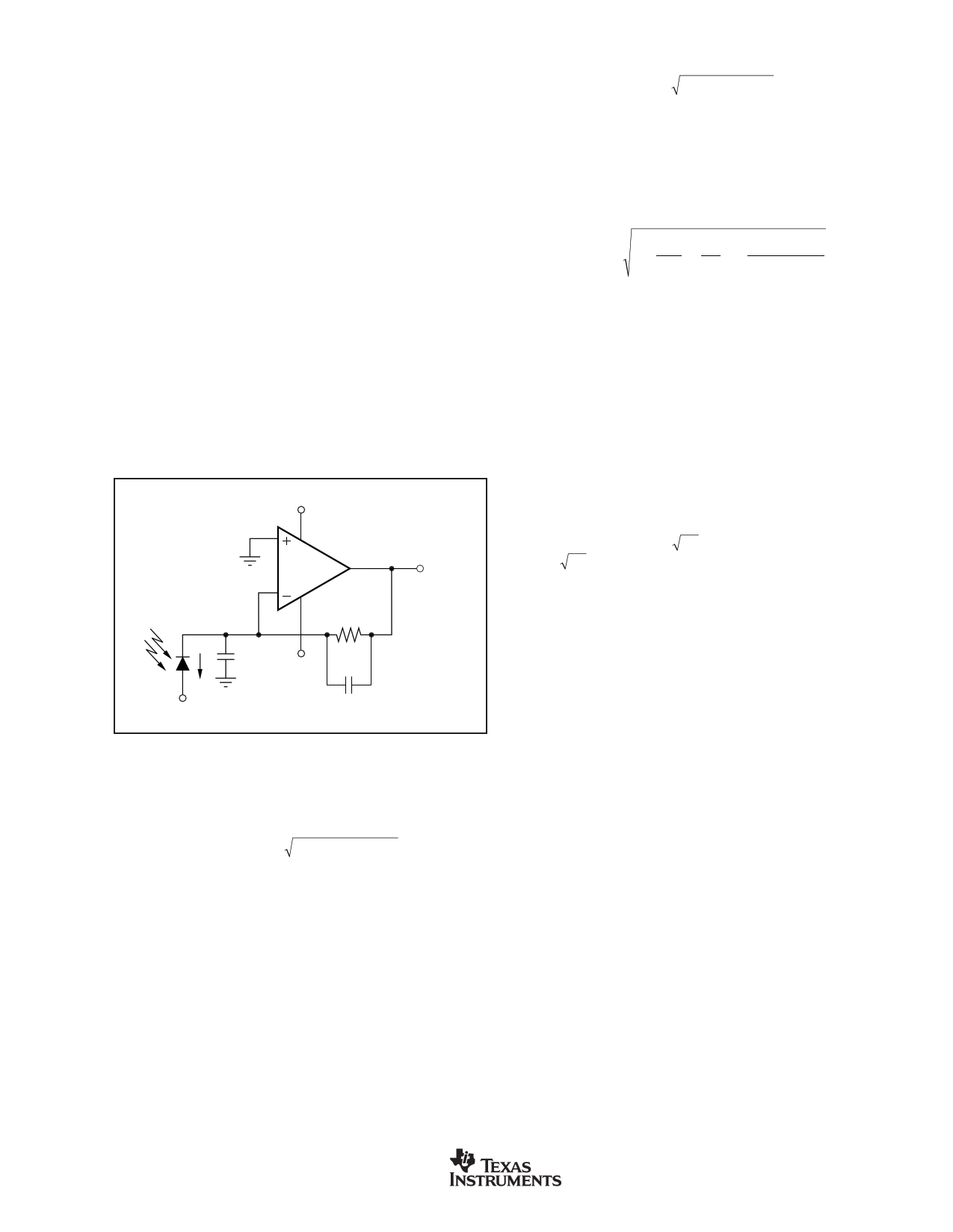
WIDEBAND, HIGH SENSITIVITY, TRANSIMPEDANCE
DESIGN
The high GBP and low input voltage and current noise for the
OPA657 make it an ideal wideband-transimpedance ampli-
fier for moderate to high transimpedance gains. Unity-gain
stability in the op amp is not required for application as a
transimpedance amplifier. One transimpedance design ex-
ample is shown on the front page of the data sheet. Designs
that require high bandwidth from a large area detector with
relatively high transimpedance gain will benefit from the low
input voltage noise for the OPA657. This input voltage noise
is peaked up over frequency by the diode source capaci-
tance, and can, in many cases, become the limiting factor to
input sensitivity. The key elements to the design are the
expected diode capacitance (CD) with the reverse bias volt-
age (–VB) applied, the desired transimpedance gain, RF, and
the GBP for the OPA657 (1600MHz). Figure 3 shows a
design from a 50pF source capacitance diode through a
200kΩ transimpedance gain. With these 3 variables set (and
including the parasitic input capacitance for the OPA657
added to CD), the feedback capacitor value (CF) may be set
to control the frequency response.
+5V
Supply Decoupling
Not Shown
OPA657
VO = ID RF
RF
200kΩ
λ
ID
CD
50pF
CF
–5V 0.2pF
–VB
FIGURE 3. Wideband, Low Noise, Transimpedance Amplifier.
To achieve a maximally flat 2nd-order Butterworth frequency
response, the feedback pole should be set to:
1/(2πRFCF ) = (GPB /(4πRFCD))
Adding the common-mode and differential mode input capaci-
tance (0.7 + 4.5)pF to the 50pF diode source capacitance of
Figure 3, and targeting a 200kΩ transimpedance gain using
the 1600MHz GBP for the OPA657 will require a feedback
pole set to 3.5MHz. This will require a total feedback capaci-
tance of 0.2pF. Typical surface-mount resistors have a para-
sitic capacitance of 0.2pF, therefore, while Figure 3 shows a
0.2pF feedback-compensation capacitor, this will actually be
the parasitic capacitance of the 200kΩ resistor.
This will give an approximate –3dB bandwidth set by:
f−3dB = GPB / 2πRFCD) Hz
The example of Figure 3 will give approximately 5MHz flat
bandwidth using the 0.2pF feedback compensation.
If the total output noise is bandlimited to a frequency less
than the feedback pole frequency, a very simple expression
for the equivalent input noise current can be derived as:
( )IEQ =
IN2
+
4kT
RF
+
EN
RF
2
+
EN 2πCDF 2
3
Where:
iEQ = Equivalent input noise current if the output noise is
bandlimited to F < 1/(2πRFCF).
iN = Input current noise for the op amp inverting input.
eN = Input voltage noise for the op amp.
CD = Diode capacitance.
F = Bandlimiting frequency in Hz (usually a postfilter prior
to further signal processing).
4kT = 1.6E – 21J at T = 290°K
Evaluating this expression up to the feedback pole frequency
at 3.9MHz for the circuit of Figure 3, gives an equivalent input
noise current of 3.4pA/ Hz. This is much higher than the
1.2fA/ Hz for just the op amp itself. This result is being
dominated by the last term in the equivalent input noise
expression. It is essential in this case to use a low voltage
noise op amp like the OPA657. If lower transimpedance gain,
wider bandwidth solutions are needed, consider the bipolar
input OPA686 or OPA687. These parts offer comparable
gain bandwidth products but much lower input noise voltage
at the expense of higher input current noise.
LOW GAIN COMPENSATION
Where a low gain is desired, and inverting operation is
acceptable, a new external compensation technique may be
used to retain the full slew rate and noise benefits of the
OPA657 while maintaining the increased loop gain and the
associated improvement in distortion offered by the decom-
pensated architecture. This technique shapes the loop gain
for good stability while giving an easily controlled 2nd-order
low-pass frequency response. Considering only the noise
gain for the circuit of Figure 4, the low-frequency noise gain,
(NG1) will be set by the resistor ratios while the high fre-
quency noise gain (NG2) will be set by the capacitor ratios.
The capacitor values set both the transition frequencies and
the high-frequency noise gain. If this noise gain, determined
by NG2 = 1 + CS/CF, is set to a value greater than the
recommended minimum stable gain for the op amp and the
noise gain pole, set by 1/RFCF, is placed correctly, a very well
controlled 2nd-order low-pass frequency response will result.
OPA657
SBOS197B
www.ti.com
11
11 Page | ||
| Páginas | Total 20 Páginas | |
| PDF Descargar | [ Datasheet OPA657.PDF ] | |
Hoja de datos destacado
| Número de pieza | Descripción | Fabricantes |
| OPA650 | Wideband Low Power Voltage Feedback Operational Amplifier | Texas Instruments |
| OPA650 | Wideband / Low Power Voltage Feedback OPERATIONAL AMPLIFIER | Burr-Brown |
| OPA651 | Wideband / Low Power Voltage Feedback OPERATIONAL AMPLIFIER | Burr-Brown |
| OPA653 | Wideband Fixed Gain JFET-Input Amplifier (Rev. A) | Texas Instruments |
| Número de pieza | Descripción | Fabricantes |
| SLA6805M | High Voltage 3 phase Motor Driver IC. |
Sanken |
| SDC1742 | 12- and 14-Bit Hybrid Synchro / Resolver-to-Digital Converters. |
Analog Devices |
|
DataSheet.es es una pagina web que funciona como un repositorio de manuales o hoja de datos de muchos de los productos más populares, |
| DataSheet.es | 2020 | Privacy Policy | Contacto | Buscar |
