|
|
PDF OP177 Data sheet ( Hoja de datos )
| Número de pieza | OP177 | |
| Descripción | Ultraprecision Operational Amplifier | |
| Fabricantes | Analog Devices | |
| Logotipo |  |
|
Hay una vista previa y un enlace de descarga de OP177 (archivo pdf) en la parte inferior de esta página. Total 17 Páginas | ||
|
No Preview Available !
Data Sheet
Ultraprecision Operational Amplifier
OP177
FEATURES
PIN CONFIGURATION
Ultralow offset voltage
TA = 25°C, 25 μV maximum
Outstanding offset voltage drift 0.3 μV/°C maximum
Excellent open-loop gain and gain linearity
12 V/μV typical
CMRR: 130 dB minimum
PSRR: 115 dB minimum
Low supply current 2.0 mA maximum
Fits industry-standard precision operational amplifier
sockets
VOS TRIM 1
–IN 2
OP177
8 VOS TRIM
7 V+
+IN 3
6 OUT
V– 4 TOP VIEW 5 NC
(Not to Scale)
NC = NO CONNECT
Figure 1. 8-Lead PDIP (P-Suffix),
8-Lead SOIC (S-Suffix)
GENERAL DESCRIPTION
The OP177 features one of the highest precision performance of
any operational amplifier currently available. Offset voltage of the
OP177 is only 25 μV maximum at room temperature. The ultralow
VOS of the OP177 combines with the exceptional offset voltage
drift (TCVOS) of 0.3 μV/°C maximum to eliminate the need for
external VOS adjustment and increases system accuracy over
temperature.
The OP177 open-loop gain of 12 V/μV is maintained over the full
±10 V output range. CMRR of 130 dB minimum, PSRR of 120 dB
minimum, and maximum supply current of 2 mA are just a few
examples of the excellent performance of this operational amplifier.
The combination of outstanding specifications of the OP177
ensures accurate performance in high closed-loop gain
applications.
This low noise, bipolar input operational amplifier is also a cost
effective alternative to chopper-stabilized amplifiers. The OP177
provides chopper-type performance without the usual problems
of high noise, low frequency chopper spikes, large physical size,
limited common-mode input voltage range, and bulky external
storage capacitors.
The OP177 is offered in the −40°C to +85°C extended industrial
temperature ranges. This product is available in 8-lead PDIP, as
well as the space saving 8-lead SOIC.
FUNCTIONAL BLOCK DIAGRAM
V+
NONINVERTING
INPUT
INVERTING
INPUT
V–
2B
Q5
R3
Q21
R4 Q22
R2A* (OPTIONAL NULL) R2B*
R1A
R1B
Q7
Q3 Q6
Q1
Q23
Q24
Q8
Q4
Q27
Q26
Q25
Q2
C1 R7
Q9
C3
R5
Q10
Q11 Q12
C2
Q14
Q13
Q19
R9
Q17
Q16
OUTPUT
R10
Q20
Q15
Q18
R6 R8
*R2A AND R2B ARE ELECTRONICALLY ADJUSTED ON CHIP AT FACTORY.
Figure 2. Simplified Schematic
Rev. H
Document Feedback
Information furnished by Analog Devices is believed to be accurate and reliable. However, no
responsibilityisassumedbyAnalogDevices for itsuse,nor foranyinfringementsofpatentsor other
rights of third parties that may result from its use. Specifications subject to change without notice. No
license is granted by implication or otherwise under any patent or patent rights of Analog Devices.
Trademarksandregisteredtrademarksarethepropertyoftheirrespectiveowners.
One Technology Way, P.O. Box 9106, Norwood, MA 02062-9106, U.S.A.
Tel: 781.329.4700 ©1995–2016 Analog Devices, Inc. All rights reserved.
Technical Support
www.analog.com
1 page 
OP177
Data Sheet
At VS = ±15 V, −40°C ≤ TA ≤ +85°C, unless otherwise noted.
Table 2.
Parameter
INPUT
Input Offset Voltage
Average Input Offset Voltage Drift1
Input Offset Current
Average Input Offset Current Drift2
Input Bias Current
Average Input Bias Current Drift2
Input Voltage Range3
COMMON-MODE REJECTION RATIO
POWER SUPPLY REJECTION RATIO
LARGE-SIGNAL VOLTAGE GAIN4
OUTPUT VOLTAGE SWING
POWER CONSUMPTION
SUPPLY CURRENT
Symbol
VOS
TCVOS
IOS
TCIOS
IB
TCIB
IVR
CMRR
PSRR
AVO
VO
PD
ISY
Test Conditions/Comments
VCM = ±13 V
VS = ±3 V to ±18 V
RL ≥ 2 kΩ, VO = ±10 V
RL ≥ 2 kΩ
VS = ±15 V, no load
VS = ±15 V, no load
OP177F
Min Typ Max
−0.2
±13
120
110
2000
±12
15
0.1
0.5
1.5
+2.4
8
±13.5
140
120
6000
±13
60
20
40
0.3
2.2
40
+4
40
75
2.5
OP177G
Min Typ Max
±13
110
106
1000
±12
20
0.7
0.5
1.5
+2.4
15
±13.5
140
115
4000
±13
60
2
100
1.2
4.5
85
±6
60
75
2.5
Unit
μV
μV/°C
nA
pA/°C
nA
pA/°C
V
dB
dB
V/mV
V
mW
mA
1 TCVOS is sample tested.
2 Guaranteed by endpoint limits.
3 Guaranteed by CMRR test condition.
4 To ensure high open-loop gain throughout the ±10 V output range, AVO is tested at −10 V ≤ VO ≤ 0 V, 0 V ≤ VO ≤ +10 V, and −10 V ≤ VO ≤ +10 V.
TEST CIRCUITS
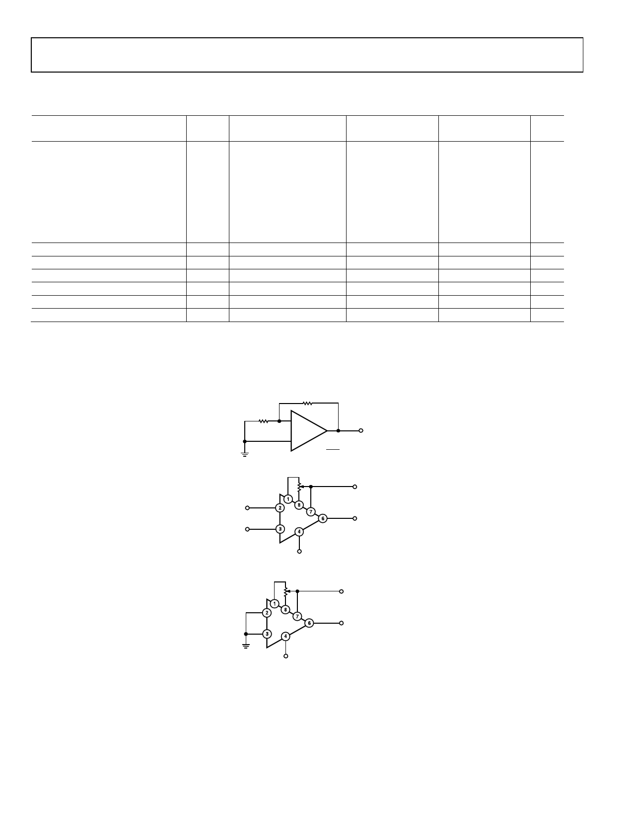
200kΩ
50Ω –
OP177
VO
+
VOS
=
VO
4000
Figure 3. Typical Offset Voltage Test Circuit
20kΩ
V+
–
INPUT
+
–
OP177
+
OUTPUT
VOS TRIM RANGE IS
TYPICALLY ±3.0mV
V–
Figure 4. Optional Offset Nulling Circuit
20kΩ
+20V
–
OP177
+
PINOUTS SHOWN FOR
P AND Z PACKAGES
–20V
Figure 5. Burn-In Circuit
Rev. H | Page 4 of 16
5 Page 
OP177
Data Sheet
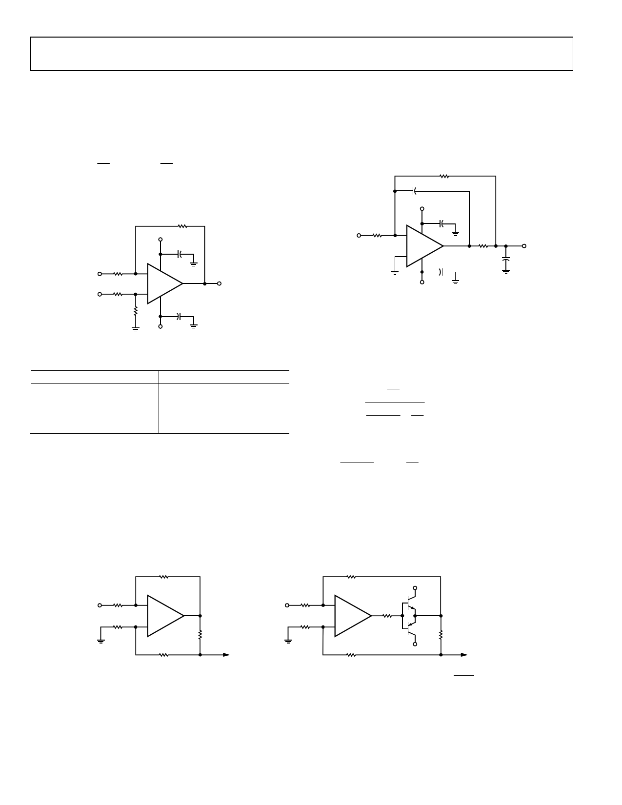
PRECISION HIGH GAIN DIFFERENTIAL AMPLIFIER
The high gain, gain linearity, CMRR, and low TCVOS of the
OP177 make it possible to obtain performance not previously
available in single stage, very high gain amplifier applications.
See Figure 28.
For best CMR, R1 must equal R3
R2 R4
In this example, with a 10 mV differential signal, the maximum
errors are listed in Table 6.
R2
1MΩ
+15V
0.1µF
R1
1kΩ
R3
1kΩ
R4
1MΩ
2– 7
OP177 6
3+
4
0.1µF
ISOLATING LARGE CAPACITIVE LOADS
The circuit shown in Figure 29 reduces maximum slew rate but
allows driving capacitive loads of any size without instability.
Because the 100 Ω resistor is inside the feedback loop, the effect
on output impedance is reduced to insignificance by the high
open loop gain of the OP177.
RF
10pF
+15V
0.1µF
INPUT
RS
2– 7
OP177 6
3 + 4 0.1µF
100Ω
OUTPUT
CLOAD
–15V
Figure 29. Isolating Capacitive Loads
BILATERAL CURRENT SOURCE
–15V
Figure 28. Precision High Gain Differential Amplifier
The current sources shown in Figure 30 supply both positive
and negative currents into a grounded load.
Table 6. High Gain Differential Amplifier Performance
Type
Amount
Common-Mode Voltage
0.1%/V
Gain Linearity, Worst Case
0.02%
TCVOS
0.0003%/°C
TCIOS
0.008%/°C
Note that
R5 R4 1
ZO
R2
R5 R4 R3
R2 R1
and that for ZO to be infinite
R5 R4 must R3
R2 R1
PRECISION ABSOLUTE VALUE AMPLIFIER
The high gain and low TCVOS assure accurate operation with
inputs from microvolts to volts. In this circuit, the signal always
appears as a common-mode signal to the operational amplifiers
(for details, see Figure 31).
BASIC CURRENT SOURCE
R3
1kΩ
R1
100kΩ
VIN
R2
100kΩ
2–
OP177
3+
6
R4
990Ω
R5
10Ω
100mA CURRENT SOURCE
R3
VIN
R1
R2
2–
OP177
3+
6 50Ω
IOUT ≤ 15mA
R4
+15V
2N2222
2N2907
–15V
R5
IOUT ≤ 100mA
Figure 30. Bilateral Current Source
IOUT
=
VIN
R3
R1 × R5
GIVEN R3 = R4 + R5, R1 = R2
Rev. H | Page 10 of 16
11 Page | ||
| Páginas | Total 17 Páginas | |
| PDF Descargar | [ Datasheet OP177.PDF ] | |
Hoja de datos destacado
| Número de pieza | Descripción | Fabricantes |
| OP176 | Bipolar/JFET / Audio Operational Amplifier | Analog Devices |
| OP177 | Ultraprecision Operational Amplifier | Analog Devices |
| OP179 | Rail-to-Rail High Output Current Operational Amplifiers | Analog Devices |
| Número de pieza | Descripción | Fabricantes |
| SLA6805M | High Voltage 3 phase Motor Driver IC. |
Sanken |
| SDC1742 | 12- and 14-Bit Hybrid Synchro / Resolver-to-Digital Converters. |
Analog Devices |
|
DataSheet.es es una pagina web que funciona como un repositorio de manuales o hoja de datos de muchos de los productos más populares, |
| DataSheet.es | 2020 | Privacy Policy | Contacto | Buscar |
